
User Guide


CHAPTER 4 IMAGE PROCESSING SYSTEM
COPYRIGHT
©
1999 CANON INC. CANON CLC1120/1130/1150 REV.0 MAR. 1999 PRINTED IN JAPAN (IMPRIME AU JAPON)
4-3
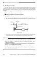
III. ANALOG IMAGE PROCESSING
The analog processor circuit performs the following on the output of the CCD:
Item Description
BGR level matching The levels of the B, G, and R signals are matched to suit the B, G,
and R offset signals to correct the rate of efficiency of photo
conversion (for B, G, and R).
Odd-/even-number bit integration The image signals of the six separate channels (according to odd-
number bits and even-number bits) are held by sample hold
signals (SH), and are integrated into image signals of three
channels (B, G, R) to suit the select signal (SEL).
A/D conversion The A/D conversion circuit converts B, G, and R image signals
into 8-bit digital signals each in sync with the ADCLK signal, and
sends the result to the image processor PCB.
Table 4-301
Figure 4-301
CCD driver
PCB
Analog processor PCB
Image processor
PCB
RGR gain, BGR offset
BGR level matching
Odd-/even-number
bit integration
To CCD
Reference pulse
generation circuit
A/D
conversion
HSYNC
(sync signal)
generation
circuit
G-ODD
G-EVEN
B-ODD
B-EVEN
R-ODD
G
B
R
G
B
R
8
8
8
R-EVEN
SH
SEL
ADCLK