
User Manual


element14 is a trademark of Premier Farnell plc 54
© 2014 Premier Farnell plc. All Rights Reserved
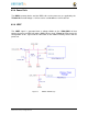
Figure 32 DDR3L Memory Design
Chip Select Line:
CS# enables (registered LOW) and disables (registered HIGH) the
command decoder. All commands are masked when CS# is registered HIGH. CS#
provides for external rank selection on systems with multiple ranks. CS# is considered
part of the command code. CS# is referenced to V
REFCA
.
Input Data Mask Line:
DM is an input mask signal for write data. Input data is masked
when DM is sampled HIGH along with the input data during a write access. Although the
DM ball is input-only, the DM loading is designed to match that of the DQ and DQS balls.
DM is referenced to VREFDQ.
On-die Termination Line:
ODT enables (registered HIGH) and disables (registered LOW)
termination resistance internal to the DDR3L SDRAM. When enabled in normal operation,
ODT is only applied to each of the following balls: DQ[7:0], DQS, DQS#, and DM for the
x8; DQ[3:0], DQS, DQS#, and DM for the x4. The ODT input is ignored if disabled via the
LOAD MODE command. ODT is referenced to VREFCA.