
Datasheet


30
2549O–AVR–05/12
ATmega640/1280/1281/2560/2561
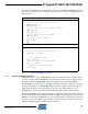
Figure 9-2. External SRAM Connected to the AVR
9.1.3 Pull-up and Bus-keeper
The pull-ups on the AD7:0 ports may be activated if the corresponding Port register is written to
one. To reduce power consumption in sleep mode, it is recommended to disable the pull-ups by
writing the Port register to zero before entering sleep.
The XMEM interface also provides a bus-keeper on the AD7:0 lines. The bus-keeper can be dis-
abled and enabled in software as described in “XMCRB – External Memory Control Register B”
on page 38. When enabled, the bus-keeper will keep the previous value on the AD7:0 bus while
these lines are tri-stated by the XMEM interface.
9.1.4 Timing
External Memory devices have different timing requirements. To meet these requirements, the
XMEM interface provides four different wait-states as shown in Table 9-3 on page 38. It is impor-
tant to consider the timing specification of the External Memory device before selecting the wait-
state. The most important parameters are the access time for the external memory compared to
the set-up requirement. The access time for the External Memory is defined to be the time from
receiving the chip select/address until the data of this address actually is driven on the bus. The
access time cannot exceed the time from the ALE pulse must be asserted low until data is stable
during a read sequence (see t
LLRL
+ t
RLRH
- t
DVRH
in Tables 31-11 through Tables 31-18 on pages
379 - 382). The different wait-states are set up in software. As an additional feature, it is possible
to divide the external memory space in two sectors with individual wait-state settings. This
makes it possible to connect two different memory devices with different timing requirements to
the same XMEM interface. For XMEM interface timing details, please refer to Table 31-11 on
page 379 to Table 31-18 on page 382 and Figure 31-9 on page 382 to Figure 31-12 on page 384
in the “External Data Memory Timing” on page 379.
Note that the XMEM interface is asynchronous and that the waveforms in the following figures
are related to the internal system clock. The skew between the internal and external clock
(XTAL1) is not guarantied (varies between devices temperature, and supply voltage). Conse-
quently, the XMEM interface is not suited for synchronous operation.
D[7:0]
A[7:0]
A[15:8]
RD
WR
SRAM
DQ
G
AD7:0
ALE
A15:8
RD
WR
AVR