
Datasheet


21
2549O–AVR–05/12
ATmega640/1280/1281/2560/2561
8. AVR Memories
This section describes the different memories in the ATmega640/1280/1281/2560/2561. The
AVR architecture has two main memory spaces, the Data Memory and the Program Memory
space. In addition, the ATmega640/1280/1281/2560/2561 features an EEPROM Memory for
data storage. All three memory spaces are linear and regular.
8.1 In-System Reprogrammable Flash Program Memory
The ATmega640/1280/1281/2560/2561 contains 64K/128K/256K bytes On-chip In-System
Reprogrammable Flash memory for program storage, see Figure 8-1. Since all AVR instructions
are 16 bit or 32 bit wide, the Flash is organized as 32K/64K/128K × 16. For software security,
the Flash Program memory space is divided into two sections, Boot Program section and Appli-
cation Program section.
The Flash memory has an endurance of at least 10,000 write/erase cycles. The
ATmega640/1280/1281/2560/2561 Program Counter (PC) is 15/16/17 bits wide, thus addressing
the 32K/64K/128K program memory locations. The operation of Boot Program section and asso-
ciated Boot Lock bits for software protection are described in detail in “Boot Loader Support –
Read-While-Write Self-Programming” on page 317. “Memory Programming” on page 335 con-
tains a detailed description on Flash data serial downloading using the SPI pins or the JTAG
interface.
Constant tables can be allocated within the entire program memory address space (see the LPM
– Load Program Memory instruction description and ELPM - Extended Load Program Memory
instruction description).
Timing diagrams for instruction fetch and execution are presented in “Instruction Execution Tim-
ing” on page 17.
8.2 SRAM Data Memory
Figure 8-2 on page 23 shows how the ATmega640/1280/1281/2560/2561 SRAM Memory is
organized.
The ATmega640/1280/1281/2560/2561 is a complex microcontroller with more peripheral units
than can be supported within the 64 location reserved in the Opcode for the IN and OUT instruc-
tions. For the Extended I/O space from $060 - $1FF in SRAM, only the ST/STS/STD and
LD/LDS/LDD instructions can be used.
The first 4,608/8,704 Data Memory locations address both the Register File, the I/O Memory,
Extended I/O Memory, and the internal data SRAM. The first 32 locations address the Register
file, the next 64 location the standard I/O Memory, then 416 locations of Extended I/O memory
and the next 8,192 locations address the internal data SRAM.
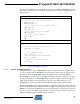
Figure 8-1. Program Flash Memory Map
Address (HEX)
0
Application Flash Section
Boot Flash Section
0x7FFF/0xFFFF/0x1FFFF