
Datasheet


ADSP-TS202S
Rev. C | Page 3 of 48 | December 2006
GENERAL DESCRIPTION
The ADSP-TS202S TigerSHARC processor is an ultrahigh per-
formance, static superscalar processor optimized for large signal
processing tasks and communications infrastructure. The DSP
combines very wide memory widths with dual computation
blocks—supporting floating-point (IEEE 32-bit and extended
precision 40-bit) and fixed-point (8-, 16-, 32-, and 64-bit) pro-
cessing—to set a new standard of performance for digital signal
processors. The TigerSHARC static superscalar architecture lets
the DSP execute up to four instructions each cycle, performing
24 fixed-point (16-bit) operations or six floating-point
operations.
Four independent 128-bit wide internal data buses, each con-
necting to the six 2M bit memory banks, enable quad-word
data, instruction, and I/O accesses and provide 28G bytes per
second of internal memory bandwidth. Operating at 500 MHz,
the ADSP-TS202S processor’s core has a 2.0 ns instruction cycle
time. Using its single-instruction, multiple-data (SIMD) fea-
tures, the ADSP-TS202S processor can perform four billion
40-bit MACS or one billion 80-bit MACS per second. Table 1
shows the DSP’s performance benchmarks.
The ADSP-TS202S processor is code-compatible with the other
TigerSHARC processors.
The Functional Block Diagram on Page 1 shows the ADSP-
TS202S processor’s architectural blocks. These blocks include
• Dual compute blocks, each consisting of an ALU, multi-
plier, 64-bit shifter, and 32-word register file and associated
data alignment buffers (DABs)
• Dual integer ALUs (IALUs), each with its own 31-word
register file for data addressing and a status register
• A program sequencer with instruction alignment buffer
(IAB) and branch target buffer (BTB)
• An interrupt controller that supports hardware and soft-
ware interrupts, supports level- or edge-triggers, and
supports prioritized, nested interrupts
• Four 128-bit internal data buses, each connecting to the six
2M-bit memory banks
• On-chip DRAM (12M-bit)
• An external port that provides the interface to host proces-
sors, multiprocessing space (DSPs), off-chip memory-
mapped peripherals, and external SRAM and SDRAM
• A 14-channel DMA controller
• Four full-duplex LVDS link ports
• Two 64-bit interval timers and timer expired pin
• An 1149.1 IEEE compliant JTAG test access port for on-
chip emulation
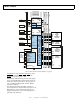
Figure 2 shows a typical single-processor system with external
SRAM and SDRAM. Figure 4 on Page 8 shows a typical multi-
processor system.
Table 1. General-Purpose Algorithm Benchmarks
at 500 MHz
Benchmark Speed
Clock
Cycles
32-bit algorithm, 1 billion MACS/s peak performance
1K point complex FFT
1
(Radix 2)
1
Cache preloaded.
18.8 μs 9419
64K point complex FFT
1
(Radix 2) 2.8 ms 1397544
FIR filter (per real tap) 1 ns 0.5
[8 × 8][8 × 8] matrix multiply (complex,
floating-point) 2.8 μs 1399
16-bit algorithm, 4 billion MACS/s peak performance
256 point complex FFT
1
(Radix 2) 1.9 μs 928
I/O DMA transfer rate
External port 1G bytes/s n/a
Link ports (each) 1G bytes/s n/a
Figure 2. ADSP-TS202S Single-Processor System with External SDRAM
BOFF
CONTROLIMP1–0
DMAR3–0
HBG
HBR
DMA DEVICE
(OPTIO NAL )
DATA
MSH
FLAG3–0
ID2–0
IOEN
RAS
CAS
LDQM
HDQM
SDWE
SDCKE
SDA10
IRQ3–0
SCLK
SCLKRAT2–0
SCLK_V
REF
V
REF
TMR0E
BM
MSSD3–0
BUSLOCK
SDRAM
MEMORY
(OPTIONAL)
CS
RAS
CAS
DQM
WE
CKE
A10
ADDR
DATA
CLK
POR_IN
JTAG
ADSP-TS202S
BMS
CLOCK
LINK
DEVICES
(4 MAX)
(OPTIONAL)
BO OT
EPROM
(OPTIO NAL)
ADDR
MEMO RY
(OPTIO NAL)
OE
DATA
ADDR
DATA
HOST
PROCESSOR
INTERFACE
(OPTIONAL)
ACK
BR7–0
CPA
MS1–0
DATA63–0
DATA
ADDR
CS
ACK
WE
ADDR31–0
D
A
T
A
C
O
N
T
R
O
L
A
D
D
R
E
S
S
BRST
REFERENCE
RD
WRH/WRL
DPA
DS2–0
CS
LxCLKINP/N
LxACKO
LxDATI3–0P/N
LxBCMPI
LxBCMPO
LxDATO3–0P/N
LxCLKOUTP/N
LxACKI
IORD
IOWR
RST_OUT
RST_IN
REFERENCE