
Datasheet


ADM2490E
Rev. A | Page 7 of 16
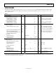
PIN CONFIGURATION AND FUNCTION DESCRIPTIONS
V
DD1
1
GND
1
2
RxD
3
NC
4
V
DD2
16
GND
2
15
A
14
B
13
GND
1
5
NC
12
TxD
6
Z
11
NC
7
Y
10
GND
1
8
GND
2
9
NC = NO CONNECT
ADM2490E
TOP VIEW
(Not to Scale)
05889-002
Figure 2. Pin Configuration
Table 9. Pin Function Descriptions
Pin No. Mnemonic Description
1 V
DD1
Power Supply (Logic Side). Decoupling capacitor to GND
1
required; capacitor value should be between
0.01 μF and 0.1 μF.
2, 5, 8 GND
1
Ground (Logic Side).
3 RxD Receiver Output.
4, 7, 12 NC No Connect. These pins must be left floating.
6 TxD Transmit Data.
9, 15 GND
2
Ground (Bus Side).
10 Y Driver Noninverting Output.
11 Z Driver Inverting Output.
13 B Receiver Inverting Input.
14 A Receiver Noninverting Input.
16 V
DD2
Power Supply (Bus Side). Decoupling capacitor to GND
2
required; capacitor value should be between
0.01 μF and 0.1 μF.