
Datasheet


ADF4360-2 Data Sheet
Rev. C | Page 20 of 24
APPLICATIONS
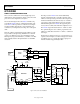
DIRECT CONVERSION MODULATOR
Direct conversion architectures are increasingly being used to
implement base station transmitters. Figure 17 shows how ADI
parts can be used to implement such a system.
The circuit block diagram shows the AD9761 TxDAC® being
used with the AD8349. The use of dual integrated DACs, such
as the AD9761 with its specified ±0.02 dB and ±0.004 dB gain
and offset matching characteristics, ensures minimum error
contribution (over temperature) from this portion of the signal
chain.
The local oscillator is implemented using the ADF4360-2. The
low-pass filter was designed using ADIsimPLL™ for a channel
spacing of 100 kHz and an open-loop bandwidth of 10 kHz.
The frequency range of the ADF4360-2 (1.85 GHz to 2.17 GHz)
makes it ideally suited for the implementation of a W-CDMA
transceiver.
The LO ports of the AD8349 can be driven differentially
from the complementary RF
OUT
A and RF
OUT
B outputs of the
ADF4360-2. This gives better performance than a single-ended
LO driver and eliminates the often necessary use of a balun to
convert from a single-ended LO input to the more desirable
differential LO inputs for the AD8349. The typical rms phase
noise (100 Hz to 100 kHz) of the LO in this configuration is 2.1°.
The AD8349 accepts LO drive levels from −10 dBm to 0 dBm.
The optimum LO power can be software programmed on the
ADF4360-2, which allows levels from −13 dBm to −6 dBm from
each output.
The RF output is designed to drive a 50 Ω load but must be ac-
coupled, as shown in Figure 17. If the I and Q inputs are driven
in quadrature by 2 V p-p signals, the resulting output power
from the modulator is approximately 2 dBm.
AD9761
TxDAC
AD8349
REFIO
FSADJ
MODULATED
DIGITAL
DATA
QOUTB
IOUTA
IOUTB
QOUTA
2kΩ
LOW-PASS
FILTER
LOW-PASS
FILTER
SPI-COMPATIBLE SERIAL BUS
ADF4360-2
V
VCO
V
VCO
V
VCO
CPGND AGND DGND
RF
OUT
B
RF
OUT
A
CP
1nF
470pF 220pF
6.8nF
47nH 47nH
1.8pF
1.8pF
100pF
TO
RF PA
3.6nH
3.6nH
1nF1nF
4.7kΩ
13kΩ
6.8kΩ
R
SET
C
C
LE
DATA
CLK
REF
IN
FREF
IN
C
N
V
TUNE
DV
DD
AV
DD
CE MUXOUT
VPS1
IBBP
IBBN
QBBP
QBBN
LOIP
LOIN
VPS2
5
4
24
7
2023221
6
14
16
17
18
19
13
1 3 8 9 10 11 22 15
12
V
DD
LOCK
DETECT
PHASE
SPLITTER
04436-021
51Ω
10µF
Figure 17. Direct Conversion Modulator