
Datasheet


ADAU1781
Rev. B| Page 15 of 92
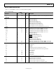
PIN CONFIGURATION AND FUNCTION DESCRIPTIONS
SDA/COUT
ADDR0/CDATA
ADDR1/CLATCH
IOVDD
DAC_SDATA/GPIO0
ADC_SDATA/GPIO1
BCLK/GPIO2
LRCLK/GPIO3
MICBIAS
BEEP
LMIC/LMICN/MICD1
LMICP
RMICP
RMIC/RMICN/MICD2
AOUTL
AOUTR
PIN 1
INDICATOR
1CM
2PDN
3AGND1
4AVDD1
5DVDDOUT
6DGND
7GPIO
8SCL/CCLK
24 NC
23 AGND2
22 SPP
21 NC
20 SPN
19 AVDD2
18 MCKO
17 MCKI
9
10
11
12
13
14
15
16
32
31
30
29
28
27
26
25
TOP VIEW
(Not to Scale)
ADAU1781
NOTES
1. NC = NO CONNECT.
2. THE EXPOSED PAD IS CONNECTED INTERNALLY TO THE
ADAU1781 GROUNDS. FOR INCREASED RELIABILITY OF THE
SOLDER JOINTS AND MAXIMUM THERMAL CAPABILITY, IT IS
RECOMMENDED THAT THE PAD BE SOLDERED TO THE
GROUND PLANE.
08314-007
Figure 7. 32-Lead LFCSP Pin Configuration
Table 10. Pin Function Descriptions
Pin No. Mnemonic Type
1
Description
1 CM A_OUT VDD/2 V Common-Mode Reference. A 10 μF to 47 μF decoupling capacitor should be
connected between this pin and ground to reduce crosstalk between the ADCs and DACs.
The material of the capacitors is not critical. This pin can be used to bias external analog
circuits, as long as they are not drawing current from CM (for example, the noninverting
input of an op amp).
2
PDN
A_IN Power-Down. Connecting this pin to GND powers down the chip. Resides in AVDD1 domain.
3 AGND1 PWR Analog Ground.
4 AVDD1 PWR Analog Power Supply. Should be equivalent to AVDD2.
5 DVDDOUT PWR Digital Core Supply Decoupling Point. The digital supply is generated from an on-board
regulator and does not require an external supply. DVDDOUT should be decoupled to DGND
with a 100 nF capacitor.
6 DGND PWR Digital Ground.
7 GPIO D_IO Dedicated General-Purpose Input/Output.
8 SCL/CCLK D_IN I
2
C Clock/SPI Clock.
9 SDA/COUT D_IO I
2
C Data/SPI Data Output.
10 ADDR0/CDATA D_IN I
2
C Address 0/SPI Data Input.
11 ADDR1/
CLATCH
D_IN I
2
C Address 1/SPI Latch Signal.
12 IOVDD PWR Supply for Digital Input and Output Pins. The digital output pins are supplied from IOVDD,
which sets the highest allowed input voltage for the digital input pins. The current draw of
this pin is variable because it is dependent on the loads of the digital outputs. IOVDD should
be decoupled to DGND with a 100 nF capacitor.
13 DAC_SDATA/GPIO0 D_IO DAC Serial Input Data/General-Purpose Input and Output.
14 ADC_SDATA/GPIO1 D_IO ADC Serial Output Data/General-Purpose Input and Output.
15 BCLK/GPIO2 D_IO Serial Data Port Bit Clock/General-Purpose Input and Output.
16 LRCLK/GPIO3 D_IO Serial Data Port Frame Clock/General-Purpose Input and Output.
17 MCKI D_IN Master Clock Input.