
Datasheet


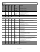


AD9979
Rev. C | Page 43 of 56
COMPLETE REGISTER LISTING
All addresses and default values are expressed in hexadecimal. When an address contains less than 28 data bits, all remaining bits must be
written as 0s.
Table 24. AFE Registers
Address
Data Bit
Content
Default
Value
Update
Type Name Description
00 [1:0] 3 SCK STANDBY Standby modes.
0 = normal operation (full power).
1 = reference standby mode.
2 = total shutdown mode (lowest power).
3 = total shutdown mode (lowest power).
[2] 1 REFBUF_PWRDN Reference buffer for REFT and REFB power control.
0 = REFT/REFB internally driven.
1 = REFT/REFB not driven.
[3] 1 CLAMPENABLE Clamp enable control.
0 = disable black clamp.
1 = enable black clamp.
[5:4] 0 TESTMODE Test operation only. Set to 0.
[6] 0 PBLK_LVL PBLK level control.
0 = blank to 0.
1 = blank to clamp level.
[7] 0 DCBYP DC restore circuit control.
0 = enable dc restore circuit during PBLK.
1 = bypass dc restore circuit during PBLK.
[9:8] 0 CDSMODE CDS operation.
0 = normal (inverting) CDS mode.
1 = sample/hold amplifier (SHA) mode.
2 = positive (noninverting) CDS mode.
3 = invalid. Do not use.
[16:10] 0 TESTMODE Test operation only. Set to 0.
[27:17] Unused Set unused bits to 0.
01 [1:0] 0 SCK TESTMODE Test operation only. Set to 0.
[2] 0 GRAYENCODE Gray coding ADC outputs.
0 = disable.
1 = enable.
[3] 0 TESTMODE Test operation only. Set to 0.
[4] 1 TESTMODE Test operation only. Set to 0.
[27:5] Unused Set unused bits to 0.
02 [0] 0 TESTMODE Test operation only. Set to 0.
[27:1] Unused Set unused bits to 0.
03 [23:0] FFFFFF TESTMODE Test operation only. Set to FFFFFF.
[27:24] Unused Set unused bits to 0.
04 [1:0] 1 VD CDSGAIN CDS gain setting.
0 = −3 dB.
1 = 0 dB (default).
2 = +3 dB.
3 = +6 dB.
[27:2] Unused Set unused bits to 0.
05 [9:0] F VD VGAGAIN VGA gain. 6 dB to 42 dB in 0.035 dB per step.
[27:10] Unused Set unused bits to 0.
06 [9:0] 1EC VD CLAMPLEVEL Optical black clamp level; 0 LSB to 1023 LSB (1 LSB per step).
[27:10] Unused Set unused bits to 0.