
Datasheet


AD9979
Rev. C | Page 37 of 56
VD
HD
CLI
XXXXXXXX
t
HDCLI
XXXXXX
t
CLISHP
t
CLIDLY
0 12
NOTES
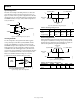
1. EXTERNAL HD FALLING EDGE IS LATCHED BY CLI RISING EDGE, THEN LATCHED AGAIN BY SHPLOC (INTERNAL SAMPLING EDGE).
2. INTERNAL H-COUNTER IS ALWAYS RESET 11.5 CLOCK CYCLES AFTER THE INTERNAL HD FALLING EDGE, AT SHDLOC (INTERNAL SAMPLING EDGE).
3. DEPENDING ON THE VALUE OF SHDLOC, H-COUNTER RESET CAN OCCUR 13 OR 14 CLI CLOCK EDGES AFTER THE EXTERNAL HD FALLING EDGE.
4. SHPLOC = 32, SHDLOC = 0 IS SHOWN IN ABOVE EXAMPLE. IN THIS CASE, THE H-COUNTER RESET OCCURS 13 CLI RISING EDGES AFTER HD FALLING EDGE.
5. HD FALLING EDGE MUST OCCUR COINCIDENT WITH VD FALLING EDGE (WITHIN SAME CLI CYCLE) OR AFTER VD FALLING EDGE. HD FALLING
EDGE MUST NOT OCCUR WITHIN 1 CLI CYCLES IMMEDIATELY BEFORE VD FALLING EDGE.
H-COUNTER
RESET
SHDLOC
INTERNAL
HD
INTERNAL
H-COUNTER
(PIXEL COUNTER)
t
VDHD
11.5 CYCLES
SHPLOC
INTERNAL
05957-055
Figure 53. Horizontal Counter Pipeline Delay
Additional Restrictions
When operating, note the following restrictions:
• The HD falling edge should be located in the same CLI
clock cycle as the VD falling edge or later than the VD
falling edge. The HD falling edge should not be located
within 1 cycle prior to the VD falling edge.
• If possible, perform all start-up serial writes with VD and
HD disabled. This prevents unknown behavior caused by
partial updating of registers before all information is loaded.
The internal horizontal counter is reset 12 CLI cycles after the
falling edge of HD. See Figure 53 for details on how the internal
counter is reset.
STANDBY MODE OPERATION
The AD9979 contains two different standby modes to optimize
the overall power dissipation in a particular application. Bits[1:0]
of Address 0x00 control the power-down state of the device.
• STANDBY[1:0] = 00 = normal operation (full power)
• STANDBY[1:0] = 01 = reference standby mode
• STANDBY[1:0] = 10 or 11 = total shut-down mode
(lowest power)
Table 22 summarizes the operation of each power-down mode.
OUT_CONTROL (Address 0x11, Bit [0]) takes priority over the
reference standby mode in determining the digital output states,
but total shutdown mode takes priority over OUT_CONTROL.
Total shutdown mode has the lowest power consumption. When
returning from total shutdown mode to normal operation, the
timing core must be reset at least 100 μs after STANDBY
(Address 0x00, Bits[1:0]) is written to.
There is an additional register to independently disable the
internal voltage reference buffer, REFBUF_PWRDN (Bit 2,
(Address 0x00). By default, the buffer is disabled. It must be
enabled for normal operation.
CLI FREQUENCY CHANGE
If the input clock (CLI) is interrupted or changes to a different
frequency, the timing core must be reset for proper operation. After
the CLI clock has settled to the new frequency, or the previous
frequency is resumed, write 0 and then 1 to TGCORE_RST
(Address 0x14). This guarantees proper timing core operation.