
Datasheet


AD9979
Rev. C | Page 35 of 56
APPLICATIONS INFORMATION
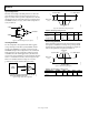
RECOMMENDED POWER-UP SEQUENCE
When the AD9979 is powered up, the following sequence is
recommended (refer to Figure 52 for each step).
1. Turn on the power supplies for the AD9979 and apply CLI
clock. There is no required order for bringing up each supply.
2. Although the AD9979 contains an on-chip, power-on reset,
a software reset of the internal registers is recommended.
Write 1 to SW_RST (Address 0x10, Bit [0], which resets all
the internal registers to their default values. This bit is self-
clearing and automatically resets back to 0.
3. Write to the desired registers to configure high speed
timing and horizontal timing. Note that all TESTMODE
registers must be written as described in the register maps.
4. To place the part into normal power operation, write 0 to
STANDBY (Address 0x00, Bits[1:0])and REFBUF_PWRDN
(Address 0x00, Bit 2).
5. The Precision Timing core must be reset by writing 1 to
TGCORE_RST (Address 0x14, Bit 0). This starts the
internal timing core operation.
6. Write 1 to OUT_CONTROL (Address 0x11, Bit 0).
The next VD/HD falling edge allows register updates to occur,
including OUT_CONTROL (Address 0x11, Bit [0]), which
enables all clock outputs.
POWER
SUPPLIES
CLI
(INPUT)
SERIAL
WRITES
VD
(INPUT)
HD
(INPUT)
HIGH-Z BY
DEFAULT
CLOCKS ACTIVE WHEN OUT_CONTROL
REGISTER IS UPDATED AT VD/HD EDGE
1H
1ST FIELD
1V
0V
AD9979 SUPPLIES
HORIZONTAL
CLOCKS
H1, H3, RG
H2, H4
4
23 5 6
1
05957-054
Figure 52. Recommended Power-Up Sequence