
Datasheet


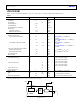


Table Of Contents
- Features
- Applications
- General Description
- Functional Block Diagram
- Revision History
- Specifications
- Absolute Maximum Ratings
- Pin Configuration and Function Descriptions
- Typical Performance Characteristics
- Terminology
- Theory of Operation
- Circuit Description
- Functional Description
- Applications Information
- Interfacing to Microprocessors
- Outline Dimensions

AD9833 Data Sheet
Rev. G | Page 6 of 21
PIN CONFIGURATION AND FUNCTION DESCRIPTIONS
COMP
1
VDD
2
CAP/2.5V
3
DGND
4
MCLK
5
VOUT
10
AGND
9
FSYNC
8
SCLK
7
SDATA
6
AD9833
TOP VIEW
(Not to Scale)
02704-005
Figure 5. Pin Configuration
Table 4. Pin Function Descriptions
Pin No. Mnemonic Description
1 COMP DAC Bias Pin. This pin is used for decoupling the DAC bias voltage.
2 VDD Positive Power Supply for the Analog and Digital Interface Sections. The on-board 2.5 V regulator is also supplied
from VDD. VDD can have a value from 2.3 V to 5.5 V. A 0.1 µF and a 10 µF decoupling capacitor should be connected
between VDD and AGND.
3 CAP/2.5V The digital circuitry operates from a 2.5 V power supply. This 2.5 V is generated from VDD using an on-board
regulator when VDD exceeds 2.7 V. The regulator requires a decoupling capacitor of 100 nF typical, which is
connected from CAP/2.5V to DGND. If VDD is less than or equal to 2.7 V, CAP/2.5V should be tied directly to VDD.
4 DGND Digital Ground.
5 MCLK Digital Clock Input. DDS output frequencies are expressed as a binary fraction of the frequency of MCLK. This
clock determines the output frequency accuracy and phase noise.
6 SDATA Serial Data Input. The 16-bit serial data-word is applied to this input.
7 SCLK Serial Clock Input. Data is clocked into the AD9833 on each falling edge of SCLK.
8 FSYNC Active Low Control Input. FSYNC
is the frame synchronization signal for the input data. When FSYNC is taken low,
the internal logic is informed that a new word is being loaded into the device.
9 AGND Analog Ground.
10 VOUT Voltage Output. The analog and digital output from the AD9833 is available at this pin. An external load resistor
is not required because the device has a 200 Ω resistor on-board.