
Datasheet


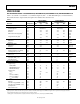


Table Of Contents
- FEATURES
- APPLICATIONS
- FUNCTIONAL BLOCK DIAGRAM
- PRODUCT HIGHLIGHTS
- TABLE OF CONTENTS
- REVISION HISTORY
- GENERAL DESCRIPTION
- SPECIFICATIONS
- ADC DC SPECIFICATIONS—AD9640ABCPZ-80, AD9640BCPZ80, AD9640ABCPZ-105, AND AD9640BCPZ-105
- ADC DC SPECIFICATIONS—AD9640ABCPZ-125, AD9640BCPZ125, AD9640ABCPZ-150, AND AD9640BCPZ150
- ADC AC SPECIFICATIONS—AD9640ABCPZ-80, AD9640BCPZ80, AD9640ABCPZ-105, AND AD9640BCPZ-105
- ADC AC SPECIFICATIONS—AD9640ABCPZ-125, AD9640BCPZ125, AD9640ABCPZ-150, AND AD9640BCPZ 150
- DIGITAL SPECIFICATIONS
- SWITCHING SPECIFICATIONS—AD9640ABCPZ-80, AD9640BCPZ-80, AD9640ABCPZ-105, AND AD9640BCPZ105
- SWITCHING SPECIFICATIONS—AD9640ABCPZ-125, AD9640BCPZ-125, AD9640ABCPZ-150, AND AD9640BCPZ150
- TIMING SPECIFICATIONS
- ABSOLUTE MAXIMUM RATINGS
- PIN CONFIGURATIONS AND FUNCTION DESCRIPTIONS
- EQUIVALENT CIRCUITS
- TYPICAL PERFORMANCE CHARACTERISTICS
- THEORY OF OPERATION
- ADC OVERRANGE AND GAIN CONTROL
- SIGNAL MONITOR
- BUILT-IN SELF-TEST (BIST) AND OUTPUT TEST
- CHANNEL/CHIP SYNCHRONIZATION
- SERIAL PORT INTERFACE (SPI)
- MEMORY MAP
- READING THE MEMORY MAP TABLE
- EXTERNAL MEMORY MAP
- MEMORY MAP REGISTER DESCRIPTION
- Sync Control (Register 0x100)
- Fast Detect Control (Register 0x104)
- Fine Upper Threshold (Register 0x106 and Register 0x107)
- Fine Lower Threshold (Register 0x108 and Register 0x109)
- Signal Monitor DC Correction Control (Register 0x10C)
- Signal Monitor DC Value Channel A (Register 0x10D and Register 0x10E)
- Signal Monitor DC Value Channel B (Register 0x10F and Register 0x110)
- Signal Monitor SPORT Control (Register 0x111)
- Signal Monitor Control (Register 0x112)
- Signal Monitor Period (Register 0x113 to Register 0x115)
- Signal Monitor Result Channel A (Register 0x116 to Register 0x118)
- Signal Monitor Result Channel B (Register 0x119 to Register 0x11B)
- APPLICATIONS INFORMATION
- OUTLINE DIMENSIONS

AD9640
Rev. B | Page 9 of 52
DIGITAL SPECIFICATIONS
AVDD = 1.8 V, DVDD = 1.8 V, DRVDD = 3.3 V, maximum sample rate, VIN = −1.0 dBFS differential input, 1.0 V internal reference, and
DCS enabled, unless otherwise noted.
Table 5.
Parameter Temperature Min Typ Max Unit
DIFFERENTIAL CLOCK INPUTS (CLK+, CLK−)
Logic Compliance CMOS/LVDS/LVPECL
Internal Common-Mode Bias Full 1.2 V
Differential Input Voltage Full 0.2 6 V p-p
Input Voltage Range Full
AGND − 0.3
AVDD + 1.6 V
Input Common-Mode Range Full 1.1 AVDD V
High Level Input Voltage Full 1.2 3.6 V
Low Level Input Voltage Full 0 0.8 V
High Level Input Current Full −10 +10 μA
Low Level Input Current Full −10 +10 μA
Input Capacitance Full 4 pF
Input Resistance Full 8 10 12 kΩ
SYNC INPUT
Logic Compliance CMOS
Internal Bias Full 1.2 V
Input Voltage Range Full AGND − 0.3 AVDD + 1.6 V
High Level Input Voltage Full 1.2 3.6 V
Low Level Input Voltage Full 0 0.8 V
High Level Input Current Full −10 +10 μA
Low Level Input Current Full −10 +10 μA
Input Capacitance Full 4 pF
Input Resistance Full 8 10 12 kΩ
LOGIC INPUT (CSB)
1
High Level Input Voltage Full 1.22 3.6 V
Low Level Input Voltage Full 0 0.6 V
High Level Input Current Full −10 +10 μA
Low Level Input Current Full 40 132 μA
Input Resistance Full 26 kΩ
Input Capacitance Full 2 pF
LOGIC INPUT (SCLK/DFS)
2
High Level Input Voltage Full 1.22 3.6 V
Low Level Input Voltage Full 0 0.6 V
High Level Input Current (VIN = 3.3 V) Full −92 −135 μA
Low Level Input Current Full −10 +10 μA
Input Resistance Full 26 kΩ
Input Capacitance Full 2 pF
LOGIC INPUTS/OUTPUTS (SDIO/DCS, SMI SDFS)
1
High Level Input Voltage Full 1.22 3.6 V
Low Level Input Voltage Full 0 0.6 V
High Level Input Current Full −10 +10 μA
Low Level Input Current Full 38 128 μA
Input Resistance Full 26 kΩ
Input Capacitance Full 5 pF
LOGIC INPUTS/OUTPUTS (SMI SDO/OEB, SMI SCLK/PDWN)
2
High Level Input Voltage Full 1.22 3.6 V
Low Level Input Voltage Full 0 0.6 V
High Level Input Current (VIN = 3.3 V) Full −90 −134 μA
Low Level Input Current Full −10 +10 μA
Input Resistance Full 26 kΩ
Input Capacitance Full 5 pF