
Datasheet


Data Sheet AD9520-0
Rev. A | Page 55 of 80
The default mode of the AD9520 serial control port is the
bidirectional mode. In bidirectional mode, both the sent data
and the readback data appear on the SDIO pin. It is also possible to
set the AD9520 to unidirectional mode (Register 0x000[7] = 1b
and Register 0x000[0] = 1b). In unidirectional mode, the readback
data appears on the SDO pin.
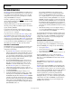
A readback request reads the data in the serial control port buffer
area or the data in the active registers (see Figure 63). Readback
of the buffer or active registers is controlled by Register 0x004[0].
The AD9520 uses Register 0x000 to Register 0xB03.
SERIAL
CONTROL
PORT
BUFFER REGISTERS
UPDATE
REGISTERS
WRITE REGISTER 0x232 = 0x001
TO UPDATE REGISTERS
ACTIVE REGISTERS
SCLK/SCL
SDO
SDIO/SDA
CS
07213-037
Figure 63. Relationship Between Serial Control Port Buffer Registers and
Active Registers of the AD9520
SPI INSTRUCTION WORD (16 BITS)
The MSB of the instruction word is R/
W
, which indicates
whether the instruction is a read or a write. The next two bits
(W1:W0) indicate the length of the transfer in bytes. The final
13 bits are the address (A12:A0) at which to begin the read or
write operation.
For a write, the instruction word is followed by the number of
bytes of data indicated by Bits[W1:W0], see Table 44.
Table 44. Byte Transfer Count
W1 W0 Bytes to Transfer
0 0 1
0 1 2
1
0
3
1 1 Streaming mode
Bits[A12:A0] select the address within the register map that is
written to or read from during the data transfer portion of the
communications cycle. For multibyte transfers, this address is
the starting byte address. In MSB first mode, subsequent bytes
decrement the address.
SPI MSB/LSB FIRST TRANSFERS
The AD9520 instruction word and byte data can be MSB first
or LSB first. Any data written to Register 0x000 must be mirrored;
the upper four bits (Bits[7:4]) must mirror the lower four bits
(Bits[3:0]). This makes it irrelevant whether LSB first or MSB
first is in effect. As an example of this mirroring, see the default
setting for Register 0x000, which mirrors Bit 4 and Bit 3. This
sets the long instruction mode, which is the default and the only
mode that is supported.
The default for the AD9520 is MSB first.
When LSB first is set by Register 0x000[1] and Register 0x000[6],
it takes effect immediately because it affects only the operation
of the serial control port and does not require that an update be
executed.
When MSB first mode is active, the instruction and data bytes
must be written from MSB to LSB. Multibyte data transfers in
MSB first format start with an instruction byte that includes the
register address of the most significant data byte. Subsequent
data bytes must follow in order from the high address to the
low address. In MSB first mode, the serial control port internal
address generator decrements for each data byte of the multibyte
transfer cycle.
When LSB first is active, the instruction and data bytes must be
written from LSB to MSB. Multibyte data transfers in LSB first
format start with an instruction byte that includes the register
address of the least significant data byte followed by multiple
data bytes. In a multibyte transfer cycle, the internal byte
address generator of the serial port increments for each byte.
The AD9520 serial control port register address decrements
from the register address just written toward Register 0x000 for
multibyte I/O operations if the MSB first mode is active
(default). If the LSB first mode is active, the register address of
the serial control port increments from the address just written
toward Register 0x232 for multibyte I/O operations.
Streaming mode always terminates when it reaches Register
0x232. Note that unused addresses are not skipped during
multibyte I/O operations.
Table 45. Streaming Mode (No Addresses Are Skipped)
Write Mode Address
Direction
Stop Sequence
LSB first Increment Register 0x230, Register 0x231,
Register 0x232, stop
MSB first Decrement Register 0x001, Register 0x000,
Register 0x232, stop
Table 46. Serial Control Port, 16-Bit Instruction Word, MSB First
MSB LSB
I15 I14 I13 I12 I11 I10 I9 I8 I7 I6 I5 I4 I3 I2 I1 I0
R/
W
W1 W0 A12 = 0 A11 = 0 A10 = 0 A9 A8 A7 A6 A5 A4 A3 A2 A1 A0