
Datasheet


AD9283
–4–
REV. C
EXPLANATION OF TEST LEVELS
Test Level
I 100% production tested.
II 100% production tested at 25°C and sample tested at
specified temperatures.
III Sample tested only.
IV Parameter is guaranteed by design and characteriza-
tion testing.
V Parameter is a typical value only.
VI 100% production tested at 25°C; guaranteed by design and
characterization testing for industrial temperature range;
100% production tested at temperature extremes for mili-
tary devices.
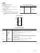
PIN CONFIGURATION
TOP VIEW
(Not to Scale)
20
19
18
17
16
15
14
13
12
11
1
2
3
4
5
6
7
8
9
10
AD9283
ENCODE
GND
V
D
VREF OUT
VREF IN
GND
A
IN
V
D
D7 (MSB)
D6
D5
D1
D2
D3
D4
V
DD
GND
PWRDWN
D0 (LSB)
A
IN
PIN FUNCTION DESCRIPTIONS
Pin Number Mnemonic Function
1 PWRDWN Power-Down Function Select; Logic HIGH for Power-Down Mode (Digital Outputs Go
to High Impedance State)
2 VREF OUT Internal Reference Output (1.25 V typ); Bypass with 0.1 µF to Ground
3 VREF IN Reference Input for ADC (1.25 V typ)
4, 9, 16 GND Ground
5, 8 V
D
Analog 3 V Power Supply
6A
IN
Analog Input for ADC (Can Be Left Open if Operating in Single-Ended Mode, but Rec-
ommend Connection to a 0.1 µF Capacitor and a 25 Ω Resistor in Series to Ground for
Better Input Matching)
7A
IN
Analog Input for ADC
10 ENCODE Encode Clock for ADC (ADC Samples on Rising Edge of ENCODE)
11–14, 17–20 D7–D4, D3–D0 Digital Outputs of ADC
15 V
DD
Digital output power supply. Nominally 2.5 V to 3.6 V
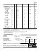
Table I. Output Coding (VREF = 1.25 V)
Step A
IN
–A
IN
Digital Output
255 0.512 1111 1111
• ••
• ••
128 0.002 1000 0000
127 –0.002 0111 1111
• ••
• ••
0 –0.512 0000 0000