
Datasheet


AD9235 Data Sheet
Rev. D | Page 8 of 40
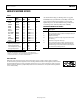
PIN CONFIGURATIONS AND FUNCTION DESCRIPTIONS
1
2
3
4
5
6
7
8
9
10
11
12
13
1
4
28
27
26
25
24
23
22
21
20
19
18
17
16
1
5
AD9235
TOP VIEW
(Not to Scale)
MODE
SENSE
VREF
AVDD
REFT
REFB
OTR
D10
D9
D8
D7
DGND
DRVDD
AGND
VIN+
VIN
–
PDWN
AVDD
AGND
D6
D5
D4
D0 (LSB)
CLK D1
D2
D3
D11 (MSB)
02461-003
Figure 3. 28-Lead TSSOP Pin Configuration
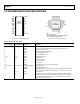
02461-004
NOTES
1. DNC = DO NOT CONNECT.
2. IT IS RECOMMENDED THAT THE EXPOSED PADDLE
BE SOLDERED TO THE GROUND PLANE.
AVDD
REFB
REFT
AVDD
AGND
VIN+
VIN–
AGND
D8
D9
D10
D11 (MSB)
OTR
MODE
SENSE
VREF
D7
DGND
DRVDD
D6
D5
D4
D3
D2
D1
D0 (LSB)
DNC
DNC
PDWN
DNC
CLK
DNC
AD9235
TOP VIEW
(Not to Scale)
1
2
3
4
5
6
7
8
24
23
22
21
20
19
18
17
9
10
11
12
13
14
15
16
32
31
30
29
28
27
26
25
Figure 4. 32-Lead LFCSP Pin Configuration
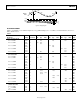
Table 6. Pin Function Descriptions
Pin No.
28-Lead TSSOP
Pin No.
32-Lead LFCSP Mnemonic Description
1 21 OTR Out-of-Range Indicator.
2 22 MODE Data Format and Clock Duty Cycle Stabilizer (DCS) Mode Selection.
3 23 SENSE Reference Mode Selection.
4 24 VREF Voltage Reference Input/Output.
5 25 REFB Differential Reference (−).
6 26 REFT Differential Reference (+).
7, 12 27, 32 AVDD Analog Power Supply.
8, 11 28, 31 AGND Analog Ground.
9 29 VIN+ Analog Input Pin (+).
10
30
VIN–
Analog Input Pin (−).
13 2 CLK Clock Input Pin.
14 4 PDWN Power-Down Function Selection (Active High).
15 to 22, 25 to 28 7 to 14, 17 to 20 D0 (LSB) to D11 (MSB) Data Output Bits.
23 15 DGND Digital Output Ground.
24 16 DRVDD Digital Output Driver Supply. Must be decoupled to DGND with a minimum.
0.1 µF capacitor. Recommended decoupling is 0.1 µF in parallel with 10 µF.
1, 3, 5, 6 DNC Do Not Connect.
EP EPAD Exposed Pad. It is recommended that the exposed paddle be soldered to the
ground plane. There is an increased reliability of the solder joints and maxi-
mum thermal capability of the package is achieved with exposed paddle
soldered to the customer board.