
Datasheet


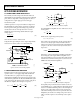
Table Of Contents
- Features
- Applications
- General Description
- Pin Configurations
- Table of Contents
- Specifications
- Absolute Maximum Ratings
- Typical Performance Characteristics
- Functional Description
- Amplifier Architecture
- Basic Auto-Zero Amplifier Theory
- High Gain, CMRR, PSRR
- Maximizing Performance Through Proper Layout
- 1/f Noise Characteristics
- Intermodulation Distortion
- Broadband and External Resistor Noise Considerations
- Output Overdrive Recovery
- Input Overvoltage Protection
- Output Phase Reversal
- Capacitive Load Drive
- Power-Up Behavior
- Applications Information
- Outline Dimensions

Data Sheet AD8551/AD8552/AD8554
Rev. E | Page 19 of 24
OUTPUT PHASE REVERSAL
Output phase reversal occurs in some amplifiers when the input
common-mode voltage range is exceeded. As common-mode
voltage moves outside of the common-mode range, the outputs
of these amplifiers suddenly jump in the opposite direction to
the supply rail. This is the result of the differential input pair
shutting down and causing a radical shifting of internal
voltages, resulting in the erratic output behavior.
The AD855x amplifiers have been carefully designed to prevent
any output phase reversal, provided both inputs are maintained
within the supply voltages. If there is the potential of one or
both inputs exceeding either supply voltage, place a resistor in
series with the input to limit the current to less than 2 mA to
ensure the output does not reverse its phase.
CAPACITIVE LOAD DRIVE
The AD855x family has excellent capacitive load driving
capabilities and can safely drive up to 10 nF from a single 5 V
supply. Although the device is stable, capacitive loading limits
the bandwidth of the amplifier. Capacitive loads also increase
the amount of overshoot and ringing at the output. An R-C
snubber network, shown in Figure 61, can be used to compensate
the amplifier against capacitive load ringing and overshoot.
5V
V
IN
200mV p-p
R
X
60Ω
C
X
0.47µF
C
L
4.7nF
V
OUT
AD8551/
AD8552/
AD8554
01101-061
Figure 61. Snubber Network Configuration for Driving Capacitive Loads
Although the snubber does not recover the loss of amplifier
bandwidth from the load capacitance, it does allow the amplifier to
drive larger values of capacitance while maintaining a minimum of
overshoot and ringing. Figure 62 shows the output of an AD855x
driving a 1 nF capacitor with and without a snubber network.
WITH
SNUBBER
WITHOUT
SNUBBER
10µs
100mV
V
SY
= 5V
C
LOAD
= 4.7nF
01101-062
Figure 62. Overshoot and Ringing are Substantially Reduced
Using a Snubber Network
The optimum value for the resistor and capacitor is a function
of the load capacitance and is best determined empirically because
actual C
LOAD
(C
L
) includes stray capacitances and may differ
substantially from the nominal capacitive load. Table 5 shows
some snubber network values that can be used as starting points.
Table 5. Snubber Network Values for Driving Capacitive Loads
C
LOAD
R
X
C
X
1 nF
200 Ω
1 nF
4.7 nF 60 Ω 0.47 μF
10 nF 20 Ω 10 μF
POWER-UP BEHAVIOR
At power-up, the AD855x settles to a valid output within 5 μs.
Figure 63 shows an oscilloscope photo of the output of the
amplifier with the power supply voltage, and Figure 64 shows
the test circuit. With the amplifier configured for unity gain, the
device takes approximately 5 μs to settle to its final output voltage.
This turn-on response time is much faster than most other
autocorrection amplifiers, which can take hundreds of
microseconds or longer for their output to settle.
V+
0V
0V
V
OUT
5µs
1V
01101-063
BOTTOM TRACE = 2V/DIV
TOP TRACE = 1V/DIV
Figure 63. AD855x Output Behavior on Power-Up
V
OUT
AD8551/
AD8552/
AD8554
V
SY
= 0V TO 5V
100kΩ
100kΩ
01101-064
Figure 64. AD855x Test Circuit for Turn-On Time