
Datasheet


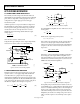
Table Of Contents
- Features
- Applications
- General Description
- Pin Configurations
- Table of Contents
- Specifications
- Absolute Maximum Ratings
- Typical Performance Characteristics
- Functional Description
- Amplifier Architecture
- Basic Auto-Zero Amplifier Theory
- High Gain, CMRR, PSRR
- Maximizing Performance Through Proper Layout
- 1/f Noise Characteristics
- Intermodulation Distortion
- Broadband and External Resistor Noise Considerations
- Output Overdrive Recovery
- Input Overvoltage Protection
- Output Phase Reversal
- Capacitive Load Drive
- Power-Up Behavior
- Applications Information
- Outline Dimensions

Data Sheet AD8551/AD8552/AD8554
Rev. E | Page 15 of 24
Amplification Phase
When the φB switches close and the φA switches open for the
amplification phase, this offset voltage remains on C
M1
and,
essentially, corrects any error from the nulling amplifier. The
voltage across C
M1
is designated as V
NA
. Furthermore, V
IN
is
designated as the potential difference between the two inputs to
the primary amplifier, or V
IN
= (V
IN+
− V
IN−
). Thus, the nulling
amplifier can be expressed as
[ ] [ ]
( )
[ ]
tVBtVtVAtV
NAAOSA
IN
AOA
−−=][
(3)
+
A
B
B
B
C
M2
V
IN+
V
NB
C
M1
V
OA
–B
A
V
NA
ФB
ФA
A
A
V
OSA
ФB
ФA
V
OUT
V
IN–
01101-051
Figure 51. Output Phase of the Amplifier
Because φA is now open and there is no place for C
M1
to discharge,
the voltage (V
NA
), at the present time (t), is equal to the voltage
at the output of the nulling amp (V
OA
) at the time when φA was
closed. If the period of the autocorrection switching frequency is
labeled t
S
, then the amplifier switches between phases every 0.5 × t
S
.
Therefore, in the amplification phase
[ ]
−=
SNANA
ttVtV
2
1
(4)
Substituting Equation 4 and Equation 2 into Equation 3 yields
[ ] [ ] [ ]
A
SOSAAA
OSAA
IN
AOA
B
ttVBA
tVAtVAtV
+
−
−+=
1
2
1
(5)
For the sake of simplification, assume that the autocorrection
frequency is much faster than any potential change in V
OSA
or
V
OSB
. This is a valid assumption because changes in offset voltage
are a function of temperature variation or long-term wear time,
both of which are much slower than the auto-zero clock frequency
of the AD855x. This effectively renders V
OS
time invariant;
therefore, Equation 5 can be rearranged and rewritten as
[ ] [ ]
( )
A
OSAAAOSAAA
IN
AOA
B
VBAVBA
tVAtV
+
−+
+=
1
1
(6)
or
[ ] [ ]
+
+=
A
OSA
IN
AOA
B
V
tVA
tV
1
(7)
From these equations, the auto-zeroing action becomes evident.
Note the V
OS
term is reduced by a 1 + B
A
factor. This shows how
the nulling amplifier has greatly reduced its own offset voltage
error even before correcting the primary amplifier. This results
in the primary amplifier output voltage becoming the voltage at
the output of the AD855x amplifier. It is equal to
[ ]
[
]
( )
NB
B
OSB
INB
OUT
VB
Vt
V
At
V +
+
=
(8)
In the amplification phase, V
OA
= V
NB
, so this can be rewritten as
[ ] [ ] [
]
+
+
++=
A
OSB
IN
A
B
OSB
BINB
OUT
B
V
tV
A
BVAtVAtV
1
(9)
Combining terms,
[ ] [ ]
( )
OSA
B
A
OSAAA
BBBIN
OUT
VA
B
VBA
BAAtVtV +
+
++=
1
(10)
The AD855x architecture is optimized in such a way that
A
A
= A
B
and B
A
= B
B
and B
A
>> 1
Also, the gain product of A
A
B
B
is much greater than A
B
. These
allow Equation 10 to be simplified to
[ ] [ ]
( )
OSBOSAAAA
IN
OUT
VVABAtVtV ++≈
(11)
Most obvious is the gain product of both the primary and nulling
amplifiers. This A
A
B
A
term is what gives the AD855x its extremely
high open-loop gain. To understand how V
OSA
and V
OSB
relate to
the overall effective input offset voltage of the complete amplifier,
establish the generic amplifier equation of
( )
EFFOS
IN
OUT
VVkV
,
+×=
(12)
where k is the open-loop gain of an amplifier and V
OS, EFF
is its
effective offset voltage.
Putting Equation 12 into the form of Equation 11 gives
[ ] [ ]
AAEFFOSAA
IN
OUT
BAVBAtVtV
,
+≈
(13)
Thus, it is evident that
A
OSBOSA
EFFOS
B
VV
V
+
≈
,
(14)
The offset voltages of both the primary and nulling amplifiers
are reduced by the Gain Factor B
A
. This takes a typical input
offset voltage from several millivolts down to an effective input
offset voltage of submicrovolts. This autocorrection scheme is
the outstanding feature of the AD855x series that continues to
earn the reputation of being among the most precise amplifiers
available on the market.