
Datasheet


AD8307
Rev. D | Page 16 of 24
It can be desirable to increase the speed of the output response,
with the penalty of increased ripple. One way to do this is by
connecting a shunt load resistor from Pin OUT to ground,
which raises the low-pass corner frequency. This also alters the
logarithmic slope, for example, to 7.5 mV/dB using a 5.36 k
resistor, while reducing the 10% to 90% rise time to 25 ns. The
ripple amplitude for the 50 MHz input remains at 0.5 mV, but
this is now equivalent to ±0.07 dB. If a negative supply is available,
the output pin can be connected directly to the summing node
of an external op amp connected as an inverting mode transresis-
tance stage.
Note that while the AD8307 can operate down to supply voltages
of 2.7 V, the output voltage limit is reduced when the supply
drops below 4 V. This characteristic is the result of necessary
headroom requirements, approximately two V
BE
drops, in the
design of the output stage.
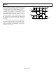
1.25kΩ
25mV/dB
OUT
2µA/dB
0µA TO 220µA
INT
FROM ALL
DETECTORS
C
FLT
C2
1pF
VPS
BIAS
1.25kΩ 1.25kΩ
~400mV
8.25kΩ
60kΩ
60µA
COM
R1
12.5kΩ
C1
2.5pF
3pF
LGP
LGM
1.25kΩ
01082-031
4
7
5
2
Figure 31. Simplified Output Interface