
Datasheet


AD8224 Data Sheet
Rev. C | Page 22 of 28
To preserve maximum pin compatibility with other dual
instrumentation amplifiers, such as the AD8222, leave the pad
unconnected. This can be done by not soldering the paddle at
all or by soldering the part to a landing that is a not connected
to any other net. For high vibration applications, a landing is
recommended.
Because the AD8224 dissipates little power, heat dissipation is
rarely an issue. If improved heat dissipation is desired (for example,
when driving heavy loads), connect the exposed pad to the
positive supply rail. For the best heat dissipation performance,
the positive supply rail should be a plane in the board. See
the Thermal Resistance section for more information.
Common-Mode Rejection over Frequency
The AD8224 has a higher CMRR over frequency than typical
in-amps, which gives it greater immunity to disturbances, such
as line noise and its associated harmonics. A well-implemented
layout is required to maintain this high performance. Input
source impedances should be matched closely. Source resistance
should be placed close to the inputs so that it interacts with as
little parasitic capacitance as possible.
Parasitics at the R
Gx
pins can also affect CMRR over frequency.
The PCB should be laid out so that the parasitic capacitances at
each pin match. Traces from the gain setting resistor to the R
Gx
pins should be kept short to minimize parasitic inductance.
Reference
Errors introduced at the reference terminal feed directly to
the output. Take care to tie the REFx pins to the appropriate
local ground.
Power Supplies
A stable dc voltage should be used to power the instrumentation
amplifier. Noise on the supply pins can adversely affect
performance.
The AD8224 has two positive supply pins (Pin 5 and Pin 16)
and two negative supply pins (Pin 8 and Pin 13). While the part
functions with only one pin from each supply pair connected,
both pins should be connected for specified performance and
optimum reliability.
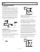
The AD8224 should be decoupled with 0.1 µF bypass capacitors,
one for each supply. Place the positive supply decoupling
capacitor near Pin 16, and the negative supply decoupling
capacitor near Pin 8. Each supply should also be decoupled with
a 10 µF tantalum capacitor. The tantalum capacitor can be
placed further away from the AD8224 and can generally be
shared by other precision integrated circuits. Figure 58 shows an
example layout.
AD8224
1
2
3
4
12
11
9
5
6
7
8
13
14
1516
0.1µF
0.1µF
R
G
R
G
10
06286-059
Figure 58. Example Layout
SOLDER WASH
The solder process can leave flux and other contaminants on
the board. When these contaminants are between the AD8224
leads and thermal pad, they can create leakage paths that are
larger than the AD8224 bias currents. A thorough washing
process removes these contaminants and restores the device’s
excellent bias current performance.
INPUT BIAS CURRENT RETURN PATH
The input bias current of the AD8224 must have a return path
to common. When the source, such as a transformer, cannot
provide a return current path, one should be created, as shown
in Figure 59.
INPUT PROTECTION
All terminals of the AD8224 are protected against ESD. ESD
protection is guaranteed to 4 kV (human body model). In addition,
the input structure allows for dc overload conditions a diode
drop above the positive supply and a diode drop below the
negative supply. Voltages beyond a diode drop of the supplies
cause the ESD diodes to conduct and enable current to flow
through the diode. Therefore, an external resistor should be
used in series with each of the inputs to limit current for
voltages beyond the supplies. In either scenario, the AD8224
safely handles a continuous 6 mA current at room temperature.