
Datasheet


AD8197B
Rev. 0 | Page 16 of 28
START
FIXED PART
ADDR
REGISTER ADDR
FIXED PART
ADDR
DATA STOP
ACK
ADDR
ACK
R/W
ADDR
ACK ACK
R/W
SR
1 2 3 4 5 6 7 8 9 10 11 12 13
I2C_SCL
GENERAL CASE
I2C_SDA
EXAMPLE
I2C_SDA
07015-029
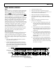
Figure 30. I
2
C Read Diagram
READ PROCEDURE
To read data from the AD8197B register set, an I
2
C master
(such as a microcontroller) needs to send the appropriate
control signals to the AD8197B slave device. The signals are
controlled by the I
2
C master, unless otherwise specified. For a
diagram of the procedure, see
Figure 30. The steps for a read
procedure are as follows:
1. Send a start condition (while holding the I2C_SCL line
high, pull the I2C_SDA line low).
2. Send the AD8197B part address (seven bits). The upper
four bits of the AD8197B part address are the static value
[1001] and the three LSBs are set by Input Pin
I2C_ADDR2, Input Pin I2C_ADDR1, and Input Pin
I2C_ADDR0 (LSB). This transfer should be MSB first.
3. Send the write indicator bit (0).
4. Wait for the AD8197B to acknowledge the request.
5. Send the register address (eight bits) from which data is to
be read. This transfer should be MSB first.
6. Wait for the AD8197B to acknowledge the request.
7. Send a repeated start condition (Sr) by holding the
I2C_SCL line high and pulling the I2C_SDA line low.
8. Resend the AD8197B part address (seven bits) from Step 2.
The upper four bits of the AD8197B part address are the
static value [1001] and the three LSBs are set by the Input
Pin I2C_ADDR2, I2C_ADDR1 and Input Pin I2C_ADDR0
(LSB). This transfer should be MSB first.
9. Send the read indicator bit (1).
10. Wait for the AD8197B to acknowledge the request.
11. The AD8197B serially transfers the data (eight bits) held in
the register indicated by the address set in Step 5. This data
is sent MSB first.
12. Acknowledge the data from the AD8197B.
13. Perform one of the following:
13a. S op condition (while holding the I2C_SCL
line high, pull the SDA line high) and release control
of the bus to end the transaction (shown in
end a st
).
13b. ted start condition (while holding the
13c.
13d. on (while holding the
SWITCH
writes to the configura-
s
tion
lly
w;
y
Figure 30
Send a repea
I2C_SCL line high, pull the I2C_SDA line low) and
continue with Step 2 of the write procedure (previous
Write Procedure section) to perform a write.
Send a repeated start condition (while holding the
I2C_SCL line high, pull the I2C_SDA line low) and
continue with Step 2 of this procedure to perform a
read from another address.
Send a repeated start conditi
I2C_SCL line high, pull the I2C_SDA line low) and
continue with Step 8 of this procedure to perform a
read from the same address.
ING/UPDATE DELAY
There is a delay between when a user
tion registers of the AD8197B and when that state change take
physical effect. This update delay occurs regardless of whether
the user programs the AD8197B via the serial or the parallel
control interface. When using the serial control interface, the
update delay begins at the falling edge of I2C_SCL for the last
data bit transferred, as shown in
Figure 29. When using the
parallel control interface, the update delay begins at the transi
edge of the relevant parallel interface pin. This update delay is
register-specific and the times are specified in
Table 1.
During a delay window, new values can be written to the
configuration registers, but the AD8197B does not physica
update until the end of that register’s delay window. Writing
new values during the delay window does not reset the windo
new values supersede the previously written values. At the end
of the delay window, the AD8197B physically assumes the state
indicated by the last set of values written to the configuration
registers. If the configuration registers are written after the dela
window ends, the AD8197B immediately updates and a new
delay window begins.