
Datasheet


AD8138
Rev. F | Page 4 of 24
V
OCM
to ±OUT SPECIFICATIONS
At 25°C, V
S
= ±5 V, V
OCM
= 0, G = +1, R
L, dm
= 500 Ω, unless otherwise noted. Refer to Figure 39 for test setup and label descriptions. All
specifications refer to single-ended input and differential outputs, unless otherwise noted.
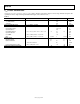
Table 2.
Parameter Conditions Min Typ Max Unit
DYNAMIC PERFORMANCE
−3 dB Bandwidth 250 MHz
Slew Rate 330 V/μs
INPUT VOLTAGE NOISE (RTI) f = 0.1 MHz to 100 MHz 17 nV/√Hz
DC PERFORMANCE
Input Voltage Range ±3.8 V
Input Resistance 200 kΩ
Input Offset Voltage V
OS, cm
= V
OUT, cm
; V
DIN+
= V
DIN–
= V
OCM
= 0 V –3.5 ±1 +3.5 mV
Input Bias Current 0.5 μA
V
OCM
CMRR ∆V
OUT, dm
/∆V
OCM
; ∆V
OCM
= ±1 V −75 dB
Gain ∆V
OUT, cm
/∆V
OCM
; ∆V
OCM
= ±1 V 0.9955 1 1.0045 V/V
POWER SUPPLY
Operating Range ±1.4 ±5.5 V
Quiescent Current 18 20 23 mA
T
MIN
to T
MAX
variation 40 μA/°C
Power Supply Rejection Ratio ∆V
OUT, dm
/∆V
S
; ∆V
S
= ±1 V −90 −70 dB
OPERATING TEMPERATURE RANGE −40 +85 °C