
Datasheet


AD8065/AD8066 Data Sheet
Rev. L | Page 20 of 28
THEORY OF OPERATION
The AD8065/AD8066 are voltage feedback operational amplifiers
that combine a laser-trimmed JFET input stage with the Analog
Devices eXtra Fast Complementary Bipolar (XFCB) process,
resulting in an outstanding combination of precision and speed.
The supply voltage range is from 5 V to 24 V. The amplifiers feature
a patented rail-to-rail output stage capable of driving within 0.5 V
of either power supply while sourcing or sinking up to 30 mA.
Also featured is a single-supply input stage that handles common-
mode signals from below the negative supply to within 3 V of the
positive rail. Operation beyond the JFET input range is possible
because of an auxiliary bipolar input stage that functions with
input voltages up to the positive supply. The amplifiers operate as
if they have a rail-to-rail input and exhibit no phase reversal
behavior for common-mode voltages within the power supply.
With voltage noise of 7 nV/√Hz and −88 dBc distortion for
1 MHz, 2 V p-p signals, the AD8065/AD8066 are a great choice
for high resolution data acquisition systems. Their low noise,
sub-pA input current, precision offset, and high speed make
them superb preamps for fast photodiode applications. The
speed and output drive capability of the AD8065/AD8066 also
make them useful in video applications.
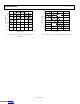
CLOSED-LOOP FREQUENCY RESPONSE
The AD8065/AD8066 are classic voltage feedback amplifiers
with an open-loop frequency response that can be approximated as
the integrator response shown in Figure 53. Basic closed-loop
frequency response for inverting and noninverting configurations
can be derived from the schematics shown.
NONINVERTING CLOSED-LOOP FREQUENCY
RESPONSE
Solving for the transfer function
( )
( )
G
crossover
G
F
F
G
crossover
I
O
Rf
sRR
RRf
V
V
××π++
+×π
=
2
2
where f
crossover
is the frequency where the amplifier’s open-loop
gain equals 0 db
At dc
G
G
F
I
O
R
RR
V
V +
=
Closed-loop −3 dB frequency
G
F
G
crossover
3dB
R
R
R
ff
+
×=
−
INVERTING CLOSED-LOOP FREQUENCY
RESPONSE
( )
G
crossover
G
F
F
crossover
I
O
R
fRRs
R
f
V
V
××
π++
××π
−
=
2
2
At dc
G
F
I
O
R
R
V
V
−=
Closed-loop −3 dB frequency
GF
G
crossoverdB
RR
R
ff
+
×=
−3
R
F
A
V
O
R
G
V
I
V
E
FREQUENCY (MHz)
80
60
0.01 100
OPEN-LOOP GAIN (A) (dB)
0.1 101
40
20
0
f
crossover
= 65MHz
A = (2π × f
crossover
)/s
R
F
V
E
A
V
O
R
G
V
I
02916-E-053
Figure 53. Open-Loop Gain vs. Frequency and Basic Connections
Downloaded from Arrow.com.Downloaded from Arrow.com.Downloaded from Arrow.com.Downloaded from Arrow.com.Downloaded from Arrow.com.Downloaded from Arrow.com.Downloaded from Arrow.com.Downloaded from Arrow.com.Downloaded from Arrow.com.Downloaded from Arrow.com.Downloaded from Arrow.com.Downloaded from Arrow.com.Downloaded from Arrow.com.Downloaded from Arrow.com.Downloaded from Arrow.com.Downloaded from Arrow.com.Downloaded from Arrow.com.Downloaded from Arrow.com.Downloaded from Arrow.com.Downloaded from Arrow.com.