
Datasheet


AD7940
Rev. A | Page 15 of 20
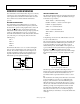
POWER VS. THROUGHPUT RATE
By using the power-down mode on the AD7940 when not
converting, the average power consumption of the ADC
decreases at lower throughput rates. Figure 19 shows how as the
throughput rate is reduced, the part remains in its shutdown
state longer, and the average power consumption over time
drops accordingly.
For example, if the AD7940 is operated in a continuous
sampling mode, with a throughput rate of 10 kSPS and an SCLK
of 2.5 MHz (V
DD
= 3.6 V), and the device is placed in power-
down mode between conversions, the power consumption is
calculated as follows. The maximum power dissipation during
normal operation is 6.84 mW (V
DD
= 3.6 V). If the power-up
time from power-down is 1 µs, and the remaining conversion
time is 6.4 µs, (using a 16 SCLK transfer), then the AD7940 can
be said to dissipate 6.84 mW for 7.4 µs during each conversion
cycle. With a throughput rate of 10 kSPS, the cycle time is 100
µs. For the remainder of the conversion cycle, 92.6 µs, the part
remains in power-down mode. The AD7940 can be said to
dissipate 1.08 µW for the remaining 92.6 µs of the conversion
cycle. Therefore, with a throughput rate of 10 kSPS, the average
power dissipated during each cycle is
(7.4/100) × (6.84 mW) + (92.6/100) × (1.08 µW) = 0.51 mW
Figure 19 shows the power dissipation versus the throughput
rate when using the power-down mode with 3.6 V supplies and
a 2.5 MHz SCLK.
03305-0-012
POWER (mW)
0.01
0 5 10 15 20 25
THROUGHPUT (kSPS)
30 35 40 45 50
0.1
1
10
V
DD
= 3.6V
F
SCLK
= 2.5MHz
Figure 19. Power vs. Throughput Using Power-Down Mode at 3.6 V