
Datasheet


AD790
REV. D
–8–
2
3
1
4
6
7
5
8
TTL
LEVEL
OUTPUT
400 *
5V
+
GND
STANDARD
SCHOTTKY
DIODE
1k
A RESISTOR UP TO 10k MAYBE USED TO
REDUCE THE SOURCE AND SINK CURRENT OF
THE DRIVER. HOWEVER, THIS WILL SLIGHTLY
LOWER THE MAXIMUM USABLE CLOCK RATE.
*
BIPOLAR
SIGNAL
INPUT
4.7V
0.3V
5V
–
Ω
Ω
Ω
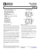
Figure 11. A Bipolar to CMOS TTL Line Receiver (N, Q
Package Pinout)
Bipolar to CMOS/TTL
It is sometimes desirable to translate a bipolar signal (e.g.,
± 5 V) coming from a communications cable or another section
of the system to CMOS/TTL logic levels; such an application is
referred to as a line receiver. Previously, the interface to the
bipolar signal required either a dual (± ) power supply or a refer-
ence voltage level about which the line receiver would switch.
The AD790 may be used in a simple circuit to provide a unique
capability: the ability to receive a bipolar signal while powered
from a single 5 V supply. Other comparators cannot perform
this task. Figure 11 shows a 1 kΩ resistor in series with the input
signal which is then clamped by a Schottky diode, holding the
input of the comparator at 0.4 V below ground. Although the
comparator is specified for a common mode range down to –V
S
,
(in this case ground) it is permissible to bring one of the inputs
a few hundred mV below ground. The comparator switches
around this level and produces a CMOS/TTL compatible swing.
The circuit will operate to switching frequencies of 20 MHz.