
Datasheet


REV. A
AD7866
–19–
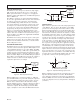
D
OUT
A. Likewise, if CS is held low for a further 16 SCLK cycles
on D
OUT
B, the data from conversion A will be output on D
OUT
B.
This is illustrated in Figure 23 where the case for D
OUT
A is shown.
Note that in this case, the D
OUT
line in use will go back into
three-state on the 32nd SCLK rising edge or the rising edge of CS,
whichever occurs first.
Sixteen serial clock cycles are required to perform the conversion
process and to access data from one conversion on either data
line of the AD7866. CS going low provides the leading zero to
be read in by the microcontroller or DSP. The remaining data is
then clocked out by subsequent SCLK falling edges, beginning
with the first of three data STATUS bits. Thus the first falling
clock edge on the serial clock has the leading zero provided and
also clocks out the first of three STATUS bits. The final bit in
the data transfer is valid on the sixteenth falling edge, having
being clocked out on the previous (fifteenth) falling edge. In
applications with a slower SCLK, it is possible to read in data on
each SCLK rising edge, i.e., the first rising edge of SCLK after
the CS falling edge would have the leading zero provided and
the fifteenth rising SCLK edge would have DB0 provided. The
three STATUS bits that follow the leading zero provide infor-
mation with respect to the conversion result that follows them
on the D
OUT
line in use. Table III shows how these identifica-
tion bits can be interpreted.
MICROPROCESSOR INTERFACING
The serial interface on the AD7866 allows the parts to be directly
connected to a range of many different microprocessors. This
section explains how to interface the AD7866 with some of the
more common microcontroller and DSP serial interface protocols.
AD7866 to ADSP-218x
The ADSP-218x family of DSPs is directly interfaced to the
AD7866 without any glue logic required. The V
DRIVE
pin of the
AD7866 takes the same supply voltage as that of the ADSP-218x.
This allows the ADC to operate at a higher supply voltage than
the serial interface, i.e., ADSP-218x, if necessary. This example
shows both D
OUT
A and D
OUT
B of the AD7866 connected to
both serial ports of the ADSP-218x.
Table III. STATUS Bit Description
Bit Bit Name Comment
15 ZERO Leading Zero. This bit will always be a zero output.
14 RANGE The polarity of this bit reflects the analog input range that has been selected with the RANGE pin.
If it is a 0, it means that in the previous transfer upon the falling edge of the CS, the range pin was
at a logic low, providing an analog input range from 0 V to V
REF
for this conversion. If it is a 1, it
means that in the previous transfer upon the falling edge of CS, the RANGE pin was at a logic high,
resulting in an analog input range of 2 V
REF
selected for this conversion. See Analog Input section.
13 A0 This bit indicates on which channel the conversion is being performed, Channel 1 or Channel 2 of
the ADC in question. If this bit is a 0, the conversion result will be from Channel 1 of the ADC;
if it is a 1, the result will be from Channel 2 of the ADC in question.
12 A/B This bit indicates from which ADC the conversion result comes. If this bit is a 0, the result is from ADC A;
if it is a 1, the result is from ADC B. This is especially useful if only one serial port is available for
use and one D
OUT
line is used, as shown in Figure 23.
The SPORT0 control register should be set up as follows:
TFSW = RFSW = 1, Alternate Framing
INVRFS = INVTFS = 1, Active Low Frame Signal
DTYPE = 00, Right Justify Data
SLEN = 1111, 16-Bit Data-Words
ISCLK = 1, Internal Serial Clock
TFSR = RFSR = 1, Frame Every Word
IRFS = 0
ITFS = 1
The SPORT1 control register should be set up as follows:
TFSW = RFSW = 1, Alternate Framing
INVRFS = INVTFS = 1, Active Low Frame Signal
DTYPE = 00, Right Justify Data
SLEN = 1111, 16-Bit Data-Words
ISCLK = 0, External Serial Clock
TFSR = RFSR = 1, Frame Every Word
IRFS = 0
ITFS = 1
To implement the power-down modes on the AD7866, SLEN
should be set to 1001 to issue an 8-bit SCLK burst. The
connection diagram is shown in Figure 24. The ADSP-218x has
the TFS0 and RFS0 of the SPORT0 and the RFS1 of SPORT1
tied together, with TFS0 set as an output and both RFS0 and RFS1
set as inputs. The DSP operates in alternate framing mode and
the SPORT control register is set up as described. The frame
synchronization signal generated on the TFS is tied to CS and,
as with all signal processing applications, equidistant sampling is
necessary. However, in this example, the timer interrupt is used to
control the sampling rate of the ADC and under certain conditions,
equidistant sampling may not be achieved.
The timer and other registers are loaded with a value that will
provide an interrupt at the required sample interval. When an
interrupt is received, a value is transmitted with TFS/DT (ADC
control word). The TFS is used to control the RFS and there-
fore the reading of data. The frequency of the serial clock is set
in the SCLKDIV register. When the instruction to transmit with
TFS is given (i.e., AX0 = TX0), the state of the SCLK is
checked. The DSP will wait until the SCLK has gone high, low,
and high before transmission will start. If the timer and SCLK
values are chosen such that the instruction to transmit occurs on
or near the rising edge of SCLK, the data may be transmitted or
it may wait until the next clock edge.