
Datasheet


AD7734 Data Sheet
Rev. A | Page 18 of 32
CHANNEL ZERO-SCALE CALIBRATION REGISTERS
24 Bits, Read/Write Registers, Address 10h–13h, Default Value
800000h
These registers hold the particular channel zero-scale
calibration coefficients. The value in these registers is used in
conjunction with the value in the corresponding channel full-
scale calibration register, the ADC zero-scale calibration
register, and the ADC full-scale register to digitally scale the
particular channel conversion results. The value in this register
is updated automatically following the execution of a channel
zero-scale system calibration.
The format of the channel zero-scale calibration register is a
sign bit and 22 bits unsigned value. Writing this register is
possible in the idle mode only (see the Calibration section for
more details).
CHANNEL FULL-SCALE CALIBRATION REGISTERS
24 Bits, Read/Write Registers, Address 18h–1Bh, Default Value
200000h
These registers hold the particular channel full-scale calibration
coefficients. The value in these registers is used in conjunction
with the value in the corresponding channel zero-scale
calibration register, the ADC zero-scale calibration register, and
the ADC full-scale register to digitally scale the particular
channel conversion results. The value in this register is updated
automatically following the execution of a channel full-scale
system calibration. Writing this register is possible in the idle
mode only (see the Calibration section for more details).
CHANNEL STATUS REGISTERS
8 Bits, Read-Only Register, Address 20h–23h, Default Value 20h × Channel Number
These registers contain individual channel status information and some general AD7734 status information. Reading the status registers
can be associated with reading the data registers in the dump mode. Reading the status registers is always associated with reading the data
registers in the continuous read mode (see the Digital Interface Description section for more details).
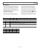
Bit Bit 7 Bit 6 Bit 5 Bit 4 Bit 3 Bit 2 Bit 1 Bit 0
Mnemonic 0 CH1 CH0 0/P0 RDY/P1 NOREF SIGN OVR
Default Channel Number 0 0 0 0 0
Bit Mnemonic Description
7–5 CH1–CH0 These bits reflect the channel n
umber. This can be used for current channel identification and easier operation
of the dump mode and continuous read mode.
4 0/P0 When the status option bit of the corresponding channel setup register is reset to 0, this bit is read as a zero.
When the status option bit is set to 1, this bit reflects the state of the P0 pin, whether it is configured as an
input or an output.
3 RDY/P1 When the status option bit of the corresponding channel setup register is reset to 0, this bit reflects the
selected channel RDY bit in the ADC status register. When the status option bit is set to 1, this bit reflects the
state of the P1 pin, whether it is configured as an input or an output.
2 NOREF This bit indicates the reference input status. If the voltage between the REFIN(+) and REFIN(–) pins is less than
NOREF, the trigger voltage and a conversion is executed, then the NOREF bit goes to 1.
1 SIGN The voltage polarity at the analog input. It will be 0 for a positive voltage and 1 for a negative voltage.
0 OVR This bit reflects either the overrange or the underrange on the analog input. The bit is set to 1 when the
analog input voltage goes over or under the nominal voltage range (see the Analog Input’s Extended Voltage
Range section).