
Datasheet


AD7734 Data Sheet
Rev. A | Page 12 of 32
PIN CONFIGURATIONS AND FUNCTIONAL DESCRIPTIONS
TOP VIEW
(Not to Scale)
28
27
26
25
24
23
22
21
20
19
18
17
16
15
1
2
3
4
5
6
7
8
9
10
11
12
13
14
AD7734
BIAS1
AIN1
AIN0
BIAS0
MUX0
INTBIAS
SYNC/P1
SCLK
MCLKIN
CS
P0
AV
DD
RESET
BIAS2
AIN2
AIN3
BIAS3
BIASLO
BIASHI
REFIN(+)
DGND
DV
DD
DIN
DOUT
REFIN(–)
AGND
RDY
MCLKOUT
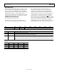
Figure 11. 28-Lead TSSOP
P0
SYNC/P1
AIN0
AIN3
AIN1
BIAS0
BIAS1
BIASHI
BIAS3
BIASLO
INTBIAS
MUX0
AIN2
BIAS2
SCLK
DIN
DOUT
CS
RESET
RDY
DGNDMCLKINMCLKOUTAGND AV
DD
DV
DD
AV
DD
DV
DD
7R
R=15.5kΩ
R
7R
R
R
7R
R
7R
7R
BUFFER
REFERENCE
DETECT
REFIN(–) REFIN(+)
AD7734
24-BIT
Σ-∆ ADC
SERIAL
INTERFACE
CONTROL
LOGIC
CLOCK
GENERATOR
CALIBRATION
CIRCUITRY
I/O PORT
MUX
Figure 12. Block Diagram
Table 10. Pin Function Descriptions—28-Lead TSSOP
Pin No. Mnemonic Description
1 SCLK Serial Clock. Schmitt triggered logic input. An external serial clock is applied to this input
to transfer serial data to or from the AD7734.
2 MCLKIN Master Clock Signal for the ADC. This can be provided in the form of a crystal/resonator
or external clock. A crystal/resonator can be tied across the MCLKIN and MCLKOUT pins.
Alternatively, the MCLKIN pin can be driven with a CMOS compatible clock and
MCLKOUT left unconnected.
3 MCLKOUT When the master clock for the device is a crystal/resonator, the crystal/resonator is
connected between MCLKIN and MCLKOUT. If an external clock is applied to the
MCLKIN, MCLKOUT provides an inverted clock signal or can be switched off to reduce
the device power consumption. MCLK OUT is capable of driving one CMOS load.
4
CS
Chip Select. Active low Schmitt triggered logic input with an internal pull-up resistor.
With this input hardwired low, the AD7734 can operate in its 3-wire interface mode
using SCLK, DIN, and DOUT.
CS
can be used to select the device in systems with more
than one device on the serial bus. It can also be used as an 8-bit frame
synchronization signal.
5
RESET
Schmitt Triggered Logic Input. Active low input that resets the control logic, interface
logic, digital filter, analog modulator, and all on-chip registers of the part to power-on
status. Effectively, everything on the part except the clock oscillator is reset when the
RESET
pin is exercised.
6 AV
DD
Analog Positive Supply Voltage. 5 V to AGND nominal.
7 P0 Digital Input/Output. The pin direction is determined by the P0 DIR bit; the digital
value can be read/written as the P0 bit in the I/O port register. The digital voltage is
referenced to analog supplies. When configured as an input, the pin should be tied
high or low.
8
SYNC
/P1
SYNC
/Digital Input/Digital Output. The pin direction is determined by the P1 DIR bit;
the
digital value can be read/written as the P1 bit in the I/O port register. When the SYNC
bit in the I/O port register is set to 1, then the
SYNC
/P1 pin can be used to synchronize
the AD7734 modulator and digital filter with other devices in the system. The digital
voltage is referenced to analog supplies. When configured as an input, the pin should be
tied high or low.