
Datasheet


AD7302
–13–
REV. 0
APPLICATIONS
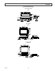
Bipolar Operation Using the AD7302
The AD7302 has been designed for single supply operation,
but bipolar operation is achievable using the circuit shown in
Figure 32. The circuit shown has been configured to achieve an
output voltage range of –5 V < V
O
< +5 V. Rail-to-rail operation
at the amplifier output is achievable using an AD820 or OP295
as the output amplifier.
The output voltage for any input code can be calculated as
follows:
V
O
= [(1+R4/R3)
×
(R2/(R1+R2)
×
(2
×
V
REF
×
D/256)] – R4
×
V
REF
/R3
where
␣␣D is the decimal equivalent of the code loaded to the DAC
and
␣␣V
REF
is the reference voltage input.
With V
REF
= 2.5 V, R1 = R3 = 10␣ kΩ and R2 = R4 = 20 kΩ and
V
DD
= 5␣ V.
V
OUT
= (10 × D/256) – 5 V
AD7302
V
OUT
A
10µF
0.1µF
V
DD
= 5V
V
DD
AGND
AD780/REF192
WITH V
DD
= 5V
OR
AD589 WITH V
DD
= 3V
REF IN
GND
V
OUT
V
IN
0.1µF
EXT REF
R1
10kΩ
R2
20kΩ
R4
20kΩ
R3
10kΩ
+5V
–5V
±5V
DGND
AD820/
OP295
Figure 32. Bipolar Operation Using the AD7302
Decoding Multiple AD7302 in a System
The CS pin on the AD7302 can be used in applications to
decode a number of DACs. In this application all DACs in the
system receive the same input data, but only the CS to one of
the DACs will be active at any one time allowing access to two
channels in the system. The 74HC139 is used as a two-to-four
line decoder to address any of the DACs in the system. To
prevent timing errors from occurring, the enable input should
be brought to its inactive state while the coded address inputs are
changing state. Figure 33 shows a diagram of a typical setup for
decoding multiple AD7302 devices in a system. The built-in
power-on reset circuit on the AD7302 ensures that the outputs
of all DACs in the system power up with zero volts on their
outputs.
AD7302
D0
D8
V
OUT
A
V
OUT
B
ENABLE
74HC139
DATA BUS
DGND
CODED
ADDRESS
1A
1B
1Y0
1Y1
1Y2
1Y3
V
CC
V
DD
1
AD7302
D0
D8
V
OUT
A
V
OUT
B
AD7302
D0
D8
V
OUT
A
V
OUT
B
AD7302
D0
D8
V
OUT
A
V
OUT
B
Figure 33. Decoding Multiple AD7302 DACs in a System
AD7302 As a Digitally Programmable Window Detector
A digitally programmable upper/lower limit detector using the
two DACs in the AD7302 is shown in Figure 34. The upper
and lower limits for the test are loaded to DACs A and B, which
in turn set the limits on the CMP04. If a signal at the V
IN
input
is not within the programmed window an LED will indicate the
fail condition.
AD7302
V
DD
+5V
V
OUT
A
DGND
REFIN
V
IN
PASS/FAIL
1/2 CMP04
1/6 74HC05
FAIL PASS
1k
0.1µF
10µF
WR
CS
A/B
1k
V
OUT
B
LDAC
CLR
DV
DD
PD
AGND
D0
D7
Figure 34. Programmable Window Detector