
Datasheet


AD7265
Rev. A | Page 24 of 28
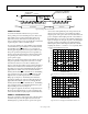
AD7265 to ADSP-BF53x AD7265 TO TMS320C541
The ADSP-BF53x family of DSPs interface directly to the
AD7265 without any glue logic required. The availability of
secondary receive registers on the serial ports of the Blackfin®
DSPs means only one serial port is necessary to read from both
D
The serial interface on the TMS320C541 uses a continuous
serial clock and frame synchronization signals to synchronize
the data transfer operations with peripheral devices like the
AD7265. The
CS
input allows easy interfacing between the
TMS320C541 and the AD7265 without any glue logic required.
The serial ports of the TMS320C541 are set up to operate in
burst mode with internal CLKX0 (TX serial clock on Serial
Port 0) and FSX0 (TX frame sync from Serial Port 0). The serial
port control registers (SPC) must have the following setup.
OUT
pins simultaneously. Figure 44 shows both D
OUT
A and
D
OUT
B of the AD7265 connected to Serial Port 0 of the
ADSP-BF53x. The SPORT0 Receive Configuration 1 register
and SPORT0 Receive Configuration 2 register should be set up
as outlined in
Table 9 and Table 10.
SERIAL
DEVICE A
(PRIMARY)
SERIAL
DEVICE B
(SECONDARY)
D
OUT
A
CS
SCLK
ADSP-BF53x
1
1
ADDITIONAL PINS OMITTED FOR CLARITY.
DR0PRI
DR0SEC
RFS0
V
DRIVE
V
DD
D
OUT
B
RCLK0
04674-037
SPORT0
AD7265
1
Table 11. Serial Port Control Register Setup
SPC FO FSM MCM TXM
SPC0 0 1 1 1
SPC1 0 1 0 0
The format bit, FO, may be set to 1 to set the word length to
8 bits to implement the power-down modes on the AD7265.
The connection diagram is shown in
Figure 45. For signal
processing applications, it is imperative that the frame
synchronization signal from the TMS320C541 provide
equidistant sampling. The V
DRIVE
pin of the AD7265 takes the
same supply voltage as that of the TMS320C541. This allows the
ADC to operate at a higher voltage than its serial interface, and
therefore, the TMS320C541, if necessary.
Figure 44. Interfacing the AD7265 to the ADSP-BF53x
Table 9. The SPORT0 Receive Configuration 1 Register
(SPORT0_RCR1)
Setting Description
FSR1
FSR0
SCLK
TMS320C541
1
1
ADDITIONAL PINS OMITTED FOR CLARITY.
CLKX0
DR1
CLKR1
CLKX1
D
OUT
B
D
OUT
A
V
DRIVE
V
DD
CS FSX0
DR0
CLKR0
04674-038
AD7265
1
RCKFE = 1 Sample data with falling edge of RSCLK
LRFS = 1 Active low frame signal
RFSR = 1 Frame every word
IRFS = 1 Internal RFS used
RLSBIT = 0 Receive MSB first
RDTYPE = 00 Zero fill
IRCLK = 1 Internal receive clock
RSPEN = 1 Receive enabled
16-bit data-word (or may be set to 1101
for 14-bit data-word)
SLEN = 1111
TFSR = RFSR = 1
Table 10. The SPORT0 Receive Configuration 2 Register
(SPORT0_RCR2)
Figure 45. Interfacing the AD7265 to the TMS320C541
Setting Description
RXSE = 1 Secondary side enabled
SLEN = 1111
16-bit data-word (or may be set to 1101
for 14-bit data-word)
To implement the power-down modes, SLEN should be set to
1001 to issue an 8-bit SCLK burst. A Blackfin driver for the
AD7265 is available to download at
www.analog.com.