
Datasheet


AD7265
Rev. A | Page 16 of 28
Using an Op Amp Pair Pseudo Differential Mode
An op amp pair can be used to directly couple a differential
signal to one of the analog input pairs of the AD7265. The
circuit configurations illustrated in
The AD7265 can have a total of six pseudo differential pairs. In
this mode, V
IN+
is connected to the signal source that must have
an amplitude of V
Figure 26 and Figure 27
show how a dual op amp can be used to convert a single-ended
signal into a differential signal for both a bipolar and unipolar
input signal, respectively.
(or 2 × V
REF REF
, depending on the range
chosen) to make use of the full dynamic range of the part. A dc
input is applied to the V
IN−
pin. The voltage applied to this input
provides an offset from ground or a pseudo ground for the V
IN+
input. The benefit of pseudo differential inputs is that they
separate the analog input signal ground from the ADC’s ground
allowing dc common-mode voltages to be cancelled. The typical
voltage range for the V
The voltage applied to Point A sets up the common-mode
voltage. In both diagrams, it is connected in some way to the
reference, but any value in the common-mode range can be
input here to set up the common mode. The
AD8022 is a
suitable dual op amp that can be used in this configuration to
provide differential drive to the AD7265.
IN−
pin, while in pseudo differential
mode, is shown in
Figure 28 and Figure 29. Figure 30 shows a
connection diagram for pseudo differential mode.
04674-043
V
REF
(V)
3.00 0.5 1.0 1.5 2.0 2.5
V
IN–
(V)
1.0
0.8
0.4
0.6
0.2
–0.2
0
–0.4
T
A
= 25°C
Take care when choosing the op amp; the selection depends on
the required power supply and system performance objectives.
The driver circuits in
Figure 26 and Figure 27 are optimized for
dc coupling applications requiring best distortion performance.
The circuit configuration shown in
Figure 26 converts a
unipolar, single-ended signal into a differential signal.
The differential op amp driver circuit shown in
Figure 27 is
configured to convert and level shift a single-ended, ground-
referenced (bipolar) signal to a differential signal centered at the
V
level of the ADC.
REF
GND
2 × V
REF
p-p
27Ω
27Ω
V+
V–
V+
V–
V
REF
2.5V
3.75V
1.25V
2.5V
3.75V
1.25V
D
CAP
A/D
CAP
B
V
IN+
V
IN–
440Ω
220Ω
0.47µF
1
ADDITIONAL PINS OMITTED FOR CLARITY.
220Ω
220Ω
10kΩ
A
04674-023
AD7265
1
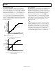
Figure 28. V
IN−
Input Voltage Range vs. V
REF
in
Pseudo Differential Mode with V
DD
= 3 V
04674-044
V
REF
(V)
5.00 0.51.01.52.02.53.03.54.04.5
V
IN–
(V)
2.5
2.0
1.5
1.0
0.5
0
–0.5
T
A
= 25°C
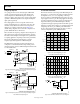
Figure 26. Dual Op Amp Circuit to Convert a Single-Ended Unipolar Signal
into a Differential Signal
20kΩ
220kΩ
2 × V
REF
p-p
27Ω
27Ω
V+
V–
V+
V–
GND
2.5V
3.75V
1.25V
2.5V
3.75V
1.25V
D
CAP
A/D
CAP
B
V
IN+
V
IN–
440Ω
220Ω
0.47µF
1
ADDITIONAL PINS OMITTED FOR CLARITY.
220Ω
220Ω
10kΩ
A
04674-024
AD7265
1
Figure 29. V
IN−
Input Voltage Range vs. V
REF
in
Pseudo Differential Mode with V
DD
= 5 V
DC INPUT
VOLTAGE
V
REF
p–p
V
REF
V
IN+
V
IN–
0.47µF
1
ADDITIONAL PINS OMITTED FOR CLARITY.
04674-025
AD7265
1
Figure 27. Dual Op Amp Circuit to Convert a Single-Ended Bipolar Signal
into a Differential Unipolar Signal
Figure 30. Pseudo Differential Mode Connection Diagram