
Datasheet


AD629
Rev. C | Page 10 of 16
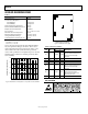
THEORY OF OPERATION
The AD629 is a unity gain, differential-to-single-ended
amplifier (diff amp) that can reject extremely high common-
mode signals (in excess of 270 V with 15 V supplies). It consists
of an operational amplifier (op amp) and a resistor network.
To achieve high common-mode voltage range, an internal
resistor divider (Pin 3 or Pin 5) attenuates the noninverting
signal by a factor of 20. Other internal resistors (Pin 1, Pin 2,
and the feedback resistor) restore the gain to provide a differential
gain of unity. The complete transfer function equals
V
OUT
= V (+IN) − V (−IN)
Laser wafer trimming provides resistor matching so that
common-mode signals are rejected while differential input
signals are amplified.
To reduce output drift, the op amp uses super beta transistors
in its input stage. The input offset current and its associated
temperature coefficient contribute no appreciable output
voltage offset or drift, which has the added benefit of reducing
voltage noise because the corner where 1/f noise becomes
dominant is below 5 Hz. To reduce the dependence of gain
accuracy on the op amp, the open-loop voltage gain of the op
amp exceeds 20 million, and the PSRR exceeds 140 dB.
1
2
3
4
8
7
6
5
21.1kΩ
380kΩ
380kΩ
380kΩ
20kΩ
REF(–)
–IN
+IN
–V
S
NC
+V
S
OUTPUT
REF(+)
AD629
NC = NO CONNECT
0
0783-001
Figure 31. Functional Block Diagram