
Datasheet


AD620
Rev. H | Page 18 of 20
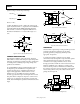
AD620ACHIPS INFORMATION
Die size: 1803 μm × 3175 μm
Die thickness: 483 μm
Bond Pad Metal: 1% Copper Doped Aluminum
To minimize gain errors introduced by the bond wires, use Kelvin connections between the chip and the gain resistor, R
G
, by connecting
Pad 1A and Pad 1B in parallel to one end of R
G
and Pad 8A and Pad 8B in parallel to the other end of R
G
. For unity gain applications
where R
G
is not required, Pad 1A and Pad 1B must be bonded together as well as the Pad 8A and Pad 8B.
1A
1B
2
3
4
5
6
7
8A
8B
LOGO
00775-0-053
Figure 49. Bond Pad Diagram
Table 6. Bond Pad Information
Pad Coordinates
1
Pad No. Mnemonic
X (μm) Y (μm)
1A R
G
−623 +1424
1B R
G
−789 +628
2 −IN −790 +453
3 +IN −790 −294
4 −V
S
−788 −1419
5 REF +570 −1429
6 OUTPUT +693 −1254
7 +V
S
+693 +139
8A R
G
+505 +1423
8B R
G
+693 +372
1
The pad coordinates indicate the center of each pad, referenced to the center of the die. The die orientation is indicated by the logo, as shown in Figure 49.