
Datasheet
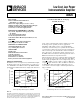


CONNECTION DIAGRAM
8-Pin Plastic Mini-DIP (N), Cerdip (Q)
and SOIC (R) Packages
–IN
R
G
–V
S
+IN
R
G
+V
S
OUTPUT
REF
1
2
3
4
8
7
6
5
AD620
TOP VIEW
REV. D
Information furnished by Analog Devices is believed to be accurate and
reliable. However, no responsibility is assumed by Analog Devices for its
use, nor for any infringements of patents or other rights of third parties
which may result from its use. No license is granted by implication or
otherwise under any patent or patent rights of Analog Devices.
a
Low Cost, Low Power
Instrumentation Amplifier
AD620
FEATURES
EASY TO USE
Gain Set with One External Resistor
(Gain Range 1 to 1000}
Wide Power Supply Range (62.3 V to 618 V)
Higher Performance than Three Op Amp IA Designs
Available in 8-Pin DIP and SOIC Packaging
Low Power, 1.3 mA max Supply Current
EXCELLENT DC PERFORMANCE (“A GRADE”)
125 mV max, Input Offset Voltage (50 mV max
“B” Grade)
1 mV/8C max, Input Offset Drift
2.0 nA max, Input Bias Current
93 dB min Common-Mode Rejection Ratio (G = 10)
LOW NOISE
9 nV/√
Hz, @ 1 kHz, Input Voltage Noise
0.28 mV p-p Noise (0.1 Hz to 10 Hz)
EXCELLENT AC SPECIFICATIONS
120 kHz Bandwidth (G = 100)
15 ms Settling Time to 0.01%
APPLICATIONS
Weigh Scales
ECG and Medical Instrumentation
Transducer Interface
Data Acquisition Systems
Industrial Process Controls
Battery Powered and Portable Equipment
One Technology Way, P.O. Box 9106, Norwood, MA 02062-9106, U.S.A.
Tel: 617/329-4700 Fax: 617/326-8703
PRODUCT DESCRIPTION
The AD620 is a low cost, high accuracy instrumentation ampli-
fier which requires only one external resistor to set gains of 1 to
1000. Furthermore, the AD620 features 8-pin SOIC and DIP
packaging that is smaller than discrete designs, and offers lower
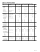
0 5 10 15 20
30,000
5,000
10,000
15,000
20,000
25,000
0
TOTAL ERROR, PPM OF FULL SCALE
SUPPLY CURRENT – mA
AD620A
R
G
3 OP-AMP
IN-AMP
(3 OP-07s)
Three Op Amp IA Designs vs. AD620
SOURCE RESISTANCE – Ω
100M10k1k 10M1M100k
10,000
0.1
100
1,000
10
1
TYPICAL STANDARD
BIPOLAR INPUT
IN-AMP
AD620 SUPERßETA
BIPOLAR INPUT
IN-AMP
RTI VOLTAGE NOISE
(0.1 –10Hz) – µV p-p
G = 100
Total Voltage Noise vs. Source Resistance
power (only 1.3 mA max supply current), making it a good fit
for battery powered, portable (or remote) applications.
The AD620, with its high accuracy of 40 ppm maximum
nonlinearity, low offset voltage of 50 µV max and offset drift of
0.6 µV/°C max, is ideal for use in precision data acquisition sys-
tems, such as weigh scales and transducer interfaces. Further-
more, the low noise, low input bias current, and low power of
the AD620 make it well suited for medical applications such as
ECG and noninvasive blood pressure monitors.
The low input bias current of 1.0 nA max is made possible with
the use of Superβeta processing in the input stage. The AD620
works well as a preamplifier due to its low input voltage noise of
9 nV/√
Hz at 1 kHz, 0.28 µV p-p in the 0.1 Hz to 10 Hz band,
0.1 pA/√
Hz input current noise. Also, the AD620 is well suited
for multiplexed applications with its settling time of 15 µs to
0.01% and its cost is low enough to enable designs with one in
amp per channel.