
Datasheet


AD600/AD602
Rev. F | Page 21
–5
–4
of 32
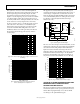
This system can, of course, be used as an AGC amplifier in
which the rms value of the input is leveled. Figure 43 shows the
decibel output voltage. More revealing is Figure 44, which
shows that the deviation from the ideal output predicted by
Equation 1 over the input range 80 V to 500 mV rms is within
±0.5 dB, and within ±1 dB for the 80 dB range from 80 V to
800 mV. By suitable choice of the input attenuator, R1 + R2, this
can be centered to cover any range from a low of 25 mV to
250 mV to a high of 1 mV to 10 V, with appropriate correction
to the value of V
REF
. Note that V
SCALE
is not affected by the
changes in the range. The gain ripple of ±0.2 dB seen in this
curve is the result of the finite interpolation error of the
X-AMP. Note that it occurs with a periodicity of 12 dB, twice
the separation between the tap points (because of the two
cascaded stages).
5
0
1
2
3
4
–3
–2
–1
10µ 100µ 101100m10m1m
INPUT SIGNAL (V rms)
2.5
0
0.5
1.0
1.5
2.0
–1.5
–1.0
–0.5
OUTPUT ER
V
OUT
(V)
00538-041
–2.5
–2.0
Figure 43. The Decibel Output of the Circuit in Figure 41 Is Linear over an
80 dB Range
R
OR (dB)
10µ 100µ 101100m10m1m
INPUT SIGNAL (V rms)
00538-042
Figure 44. Data from Figure 42 Presented as the Deviation
from the Ideal Output Given in Equation 4
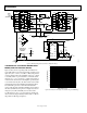
This ripple can be canceled whenever the X-AMP stages are
cascaded by introducing a 3 dB offset between the two pairs of
control voltages. A simple means to achieve this is shown in
Figure 45: the voltages at C1HI and C2HI are split by ±46.875 mV,
or ±1.5 dB. Alternatively, either one of these pins can be offset
by 3 dB and a 1.5 dB gain adjustment made at the input
attenuator (R1 + R2).
16
15
14
13
12
11
10
9
U1
AD600
C1HI
A1CM
A1OP
VPOS
VNEG
A2OP
A2CM
C2HI
1
2
3
4
5
6
7
V
IN
–V
S
C
AV
dB
BUF OUT
BUF IN
U2
+6V DEC
–6V DEC
C2
2µF
A
D636
NC
NC
NC
–6V DEC
–46.875mV
NC = NO CONNECT
10kΩ
10kΩ
+6V
DEC
–6V
DEC
78.7Ω 78.7Ω
3dB OFFSET
MODIFICATION
+46.875mV
00538-043
2.5
0
–2.5
0.5
1.0
1.5
2.0
–2.0
–1.5
–1.0
–0.5
OUTPUT ERROR (dB)
10µ 100µ 101100m10m1m
INPUT SIGNAL (V rms)
Figure 45. Reducing the Gain Error Ripple
The error curve shown in Figure 46 demonstrates that, over the
central portion of the range, the output voltage can be maintained
close to the ideal value. The penalty for this modification is
higher errors at the extremities of the range. The next two
applications show how three amplifier sections can be cascaded
to extend the nominal conversion range to 120 dB, with the
inclusion of simple LP filters of the type shown in Figure 37.
Very low errors can then be maintained over a 100 dB range.
00538-044
Figure 46. Using a 3 dB Offset Network Reduces Ripple
100 dB TO 120 dB RMS RESPONDING CONSTANT
BANDWIDTH AGC SYSTEMS WITH HIGH
ACCURACY DECIBEL OUTPUTS
The next two applications double as both AGC amplifiers and
measurement systems. In both, precise gain offsets are used to
achieve either a high gain linearity of ±0.1 dB over the full
100 dB range or the optimal SNR at any gain.