
Datasheet


AD5626
Rev. A | Page 14 of 20
CS
CLR
SCLK
LDAC
SDIN
2
8
6
5
3
4
V
OUT
1
7
V
DD
GND
AD5626
0.1µF
10µF
+5
V
+5V
+
A2
8
4
5
7
6
R1
10k
R2
12.7k
P1
10k
R3
247k
2.5V
TRIM
ZERO-SCALE
ADJUST
–2.5V
–5V
–5V V
O
+5
V
+
–
R4
23.7k
FULL-SCALE
ADJUST
P3
500
P2
10k
A1
3
1
2
100
A1, A2 = 1/2 OP295
–2.5V
+
–
+5V
0.1µF
ADR03
2
4
6
5
0.01µF
06757-030
Figure 30. Bipolar Output Operation
06757-031
CS
CLR
SCLK
LDAC
SDIN
2
8
6
5
3
4
V
OUT
1
7
V
DD
GND
AD5626
+5V
0.1µF
+5V
+2.5V
A1
8
4
3
1
2
R3
R4
–5V
V
O
+
–
R2
+5
V
0.1µF
ADR03
2
4
6
R1
±2.5V
±5V
15k + 274
R1
10k
10k 43.2k + 499
10k
20k
R2
1
0
k
1
0
k
R
3
R4V
OUT
RANGE
A1 = 1/2 OP295
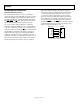
Figure 31. Bipolar Output Operation Without Trim
Table 7. Bipolar Code
Hexadecimal Number
in DAC Register
Decimal Number
in DAC Register
Analog Output
Voltage (V)
FFF 4095 −4.9976
801 2049 −2.44E − 3
800 2048 0
7FF 2047 +2.44E − 3
000 0 +5
To maintain monotonicity and accuracy, R1, R2, and R4 should
be selected to match within 0.01% and must all be of the same
(preferably metal foil) type to assure temperature coefficient
matching. Mismatching between R1 and R2 causes offset and
gain errors whereas an R4 to R1 or R4 to R2 mismatch yields
gain errors.
For applications that do not require high accuracy, the circuit
illustrated in Figure 31 can also be used to generate a bipolar
output voltage. In this circuit, only one op amp is used and no
potentiometers are used for offset and gain trim. The output
voltage is coded in offset binary and is given by
R1
R2
R1
R2
R4R3
R4
CodeDigitalV
O
×−
⎟
⎠
⎞
⎜
⎝
⎛
+×
⎟
⎠
⎞
⎜
⎝
⎛
+
××= 5.21mV1