
Datasheet


AS4C8M16SA
Confidential
12
Rev. 2.2 Mar /2014
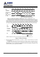
CLK
DQ
T0 T1 T2 T3 T4 T5 T6
DIN A
0
DIN A
1
T7 T8
COMMAND
Bank A
Activate
NOP NOP
WRITE A
Auto Precharge
NOP NOP NOP NOP NOP
T9
Bank A
Activate
t
DAL
=t
WR
+t
RP
t
DAL
Begin AutoPrecharge
Bank can be reactivated at
completion of t
DAL
Figure 14. Burst Write with Auto-Precharge
(Burst Length = 2)
8 Mode Register Set command
(RAS# = "L", CAS# = "L", WE# = "L", A0-A11 = Register Data)
The mode register stores the data for controlling the various operating modes of SDRAM. The Mode
Register Set command programs the values of CAS latency, Addressing Mode and Burst Length in the
Mode register to make SDRAM useful for a variety of different applications. The default values of the
Mode Register after power-up are undefined; therefore this command must be issued at the power-up
sequence. The state of pins A0~A9 and A11 in the same cycle is the data written to the mode register.
Two clock cycles are required to complete the write in the mode register (refer to the following figure). The
contents of the mode register can be changed using the same command and the clock cycle
requirements during operation as long as all banks are in the idle state.
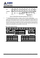
Table 5. Mode Register Bitmap
BA0,1
A11,A10
A9
A8
A7
A6
A5
A4
A3
A2
A1
A0
RFU*
RFU*
WBL
Test Mode
CAS Latency
BT
Burst Length
A9
Write Burst Length
A8
A7
Test Mode
A3
Burst Type
0
Burst
0
0
Normal
0
Sequential
1
Single Bit
1
0
Vendor Use Only
1
Interleave
0
1
Vendor Use Only
A6
A5
A4
CAS Latency
A2
A1
A0
Burst Length
0
0
0
Reserved
0
0
0
1
0
0
1
Reserved
0
0
1
2
0
1
0
2 clocks
0
1
0
4
0
1
1
3 clocks
0
1
1
8
1
0
0
Reserved
1
1
1
Full Page (Sequential)
All other Reserved
All other Reserved
*Note: RFU (Reserved for future use) should stay “0” during MRS cycle.