
User guide


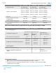


Figure 2-88: Use ATX PLL or fPLL for Gen1/Gen2/Gen3 x8 Mode
CDR
CGB
Ch 4
CDR
CGB
Ch 3
CDR
CGB
Ch 2
CDR
CGB
Ch 1
CDR
CGB
Ch 0
CDR
CGB
Ch 5
6
6
6
6
Master
CGB
6
6Master
CGB
ATX PLL1
fPLL1
Connections Done
via X1 Network
Notes:
1. The figure shown is just one possible combination for the PCIe Gen1/Gen2/Gen3 x8 mode.
2. The x6 and xN clock networks are used for channel bonding applications.
3. Each master CGB drives one set of x6 clock lines. The x6 lines further drive the xN lines.
4. Gen1/Gen2 x8 modes use the fPLL only.
5. Gen3 mode uses the ATX PLL only.
6. Use the pll_pcie_clk from the fPLL, configured as Gen1/Gen2. This is the hclk required by the PIPE interface.
CDR
CGB
Ch 5
CDR
CGB
Ch 4
Transceiver
bank
6
Master
CGB
Transceiver
bank
Related Information
• Using PLLs and Clock Networks on page 3-49
For more information about implementing clock configurations and configuring PLLs.
• PIPE Design Example
For more information about the PLL configuration for PCIe.
2-244
How to Connect TX PLLs for PIPE Gen1, Gen2, and Gen3 Modes
UG-01143
2015.05.11
Altera Corporation
Implementing Protocols in Arria 10 Transceivers
Send Feedback