
Datasheet


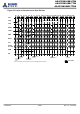


Table 16. Electrical Characteristics and Recommended A.C. Operating Conditions
(V
DD
= 3.3V
±
0.3V, T
A
= -40~85°C) (Note: 5, 6, 7, 8)
Symbol
A.C. Parameter
-6
-7
Unit
Note
Min.
Max.
Min.
Max.
t
RC
Row cycle time (same bank)
60
-
63
-
ns
t
RFC
Refresh cycle time
60
-
63
-
t
RCD
RAS# to CAS# delay (same bank)
18
-
21
-
t
RP
Precharge to refresh/row activate command
(same bank)
18
-
21
-
t
RRD
Row activate to row activate delay
(different banks)
12
-
14
-
t
MRD
Mode register set cycle time
12
-
14
-
t
RAS
Row activate to precharge time (same bank)
42
120K
42
120K
t
WR
Write recovery time
12
-
14
-
t
CK
Clock cycle time
CL* = 2
10
-
10
-
9
CL* = 3
6
-
7
-
t
CH
Clock high time
2
-
2.5
-
10
t
CL
Clock low time
2
-
2.5
-
10
t
AC
Access time from CLK
(positive edge)
CL* = 2
-
6
-
6
10
CL* = 3
-
5
-
5.4
t
OH
Data output hold time
2.5
-
2.5
-
9
t
LZ
Data output low impedance
0
-
0
-
t
HZ
Data output high impedance
-
5
-
5.4
8
t
IS
Data/Address/Control Input set-up time
1.5
-
1.5
-
10
t
IH
Data/Address/Control Input hold time
0.8
-
0.8
-
10
t
PDE
Power Down Exit set-up time
t
IS+
t
CK
-
t
IS+
t
CK
-
t
REFI
Average Refresh interval time
-
7.8
-
7.8
μs
t
XSR
Exit Self-Refresh to any Command
t
RC+
t
IS
-
t
RC+
t
IS
-
ns
*
CL is CAS Latency.
Note:
1. Stress greater than those listed under "Absolute Maximum Ratings" may cause permanent damage to the
device. Absolute maximum DC requirements contain stress ratings only. Functional operation at the
absolute maximum limits is not implied or guaranteed. Extended exposure to maximum ratings may affect
device reliability.
2. All voltages are referenced to V
SS
. Overshoot V
IH
(Max) = 4.6V for pulse width ≤ 3ns. Undershoot V
IL
(Min) = -1.0V
for pulse width ≤ 3ns.
3. These parameters depend on the cycle rate and these values are measured by the cycle rate under the
minimum value of t
CK
and t
RC
. Input signals are changed one time during every 2 t
CK
.
4. These parameters depend on the output loading. Specified values are obtained with the output open.
5. Power-up sequence is described in Note 11.
6. A.C. Test Conditions
AS4C32M16SB-6TIN
AS4C32M16SB-7TIN
AS4C32M16SB-7TCN
Confidential
- 21/55 -
Rev.1.0 June 2016