cover1 3/27/95 9:57 AM Page 1 8mm CAMCORDER SERVICE MANUAL VP-A30/SCA30 VP-A31/SCA33 VP-A33/SCA35 VP-A34/SCA80 VP-A800/SCA85 VP-A850 SCA30/SCA33/SCA35/SCA80/SCA85/VP-A30VP-A31/VP-A33/VP-A34/VP-A800/VP-A850 © Samsung Electronics Co.,Ltd. MAR. 1999 Printed in Korea AD68-00079A SERVICE Manual For mechanical disassembly and adjustment, refer to the “Mechanical Manual” (DE-6 AD68-30200A). 8mm CAMCORDER CONTENTS 1. Precautions 2. Service Tips 3. Product Specifications and Comparison Chart 4.
1. Precautions 1. Be sure that all of the built-in protective devices are replaced. Restore any missing protective shields. 2. When reinstalling the chassis and its assemblies, be sure to restore all protective devices, including : control knobs and compartment covers. 3. Make sure that there are no cabinet openings through which people--particularly children --might insert fingers and contact dangerous voltages.
Precautions 11. High voltage is maintained within specified limits by close-tolerance, safety-related components and adjustments. If the high voltage exceeds the specified limits, check each of the special components. 12. Design Alteration Warning : Never alter or add to the mechanical or electrical design of this unit. Example : Do not add auxiliary audio or video connectors. Such alterations might create a safety hazard. Also, any design changes or additions will void the manufacturer’s warranty. 13.
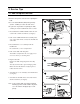
2. Service Tips 2-1 How to replace the bulb ✤ Remove the power source before replacing the bulb. ✤ Use the JC6V-3W/G4 (100H) halogen lamp (maker : USHIO) to reduce the disk of fire. PUSH ✤ If you have any trouble in replacing the bulb, contact you nearest authorized service center. 1. Disassemble the VIDEO LIGHT unit from camcorder with a small screwdriver (see figure). 2. Pull out the VIDEO LIGHT unit carefully. Take care of the cable which connects the LIGHT and camcorder. 3.
3. Product Specifications and Comparison Chart 3-1 NTSC Model (SCA30/SCA33/SCA35/SCA80/SCA85) System Recording system SCA30/SCA33/SCA35/SCA80/SCA85 Video: 2 rotary heads helical scanning FM Audio: FM monaural system (SCA80/SCA85: FM stereo) Video signal NTSC color, EIA standard Usable cassette SCA30/SCA33/SCA35: 8 mm SCA80/SCA85: Hi8 or 8 mm Tape speed SP: approx. 14.345 mm/sec Speed mode Record: SP only Recording time P6-120: 120 min FF or REW time P6-120: approx. 6.5 min.
Products Specifications 3-2 PAL Model (VP-A30/VP-A31/VP-A33/VP-A34/VP-A800/VP-A850 System Recording system VP-A30/VP-A31/VP-A33/VP-A34/VP-A800/VP-A850 Video: 2 rotary heads helical scanning FM Audio: FM monaural system (VP-A800/A850: FM stereo) Video signal PAL colour, CCIR standard Usable cassette VP-A30/VP-A31/VP-A33/VP-A34: 8 mm VP-A800/VP-A850: Hi8 or 8 mm Tape speed SP: approx. 20.051 mm/sec Speed mode Record: SP only Recording time P5-90: 90 min. FF or REW time P5-90: approx. 8 min.
Precautions 3-3 Comparison Chart Model PAL VP-A30 VP-A31 VP-A33 VP-A34 VP-A800 VP-A850 V/Light X X X O X O BLC O O O O O O EIS X X X O X O WDR X O O O O O Remocon X O O O O O Battery Ni-cd Ni-MH Ni-MH Ni-MH Ni-MH Ni-MH Audio Mono Mono Mono Mono Stereo Stereo V/Finder EVF EVF CVF EVF EVF EVF P.
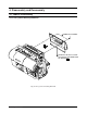
4. Disassembly and Reassembly 4-1 Cabinet Disassembly 4-1-1 Ass’y Cover Housing Removal 1 REMOVE 2 SCREWS. A 2 REMOVE THE ASS'Y COVER HOUSING IN THE DIRECTION OF ARROW. A Fig.
Disassemblr and Reassembly 4-1-2 Ass’y Case Top Removal 1 REMOVE ASS'Y CASE TOP BY GENTLELY RELEASING 2 LOCKING TABS WITH A SMALL SCREW DRIVER. (SEE DETAIL "A") REASSEMBLY : PUT THE 7 TABS INTO THE SLOT, WHILE SLIDING IT AS SHOWN IN DETAIL "B". 2 LOCKING TABS "B" PRECISION SCREW DRIVER < DETAIL "B" > < DETAIL "A" > Fig.
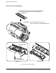
Disassemblr and Reassembly 4-1-3 Ass’y Front Removal 2 REMOVE THE ASS'Y FRONT IN THE DIRECTION OF ARROW. A B 1 A 1 1 3 REMOVE 4 SCREWS. B DISCONNECT THE FPC FROM THE CN702 OF ASS'Y AUDIO BOARD. 1 Fig.
Disassemblr and Reassembly 4-1-4 Ass’y Case Right Removal REMOVE THE UNIT CASE IN THE DIRECTION OF ARROW. A 2 1 REMOVE 3 SCREWS. A DISASSEMBLE AFTER TURNING KNOB to be "LOCK". 1 1 Fig.
Disassemblr and Reassembly 4-1-5 Ass’y Case Left Removal 4 REMOVE THE CASE LEFT ASSEMBLY IN THE DIRECTION OF ARROW. A 2 A 1 2 3 REMOVE 2 SCREWS. REMOVE 2 SCREWS. REMOVE 1 SCREWS. Fig.
Disassemblr and Reassembly 4-1-6 Ass’y EVF/CVF Removal Caution of assembling (CN604 of the CVF models) : Insert the cable to the left most side of CN604 (Pin no.1 side) 1 2 REMOVE 2 SCREWS. REMOVE 3 SCREWS. 2 A 3 REMOVE THE EVF/CVF ASS'Y IN THE DIRECTION OF ARROW. A Fig.
Disassemblr and Reassembly 4-1-7 Ass’y Function Board Removal 1 REMOVE 1 SCREW. 3 REMOVE THE ASS'Y FUNCTION BOARD IN THE DIRECTION OF ARROW. A A 2 REMOVE 1 SCREW. Fig.
Disassemblr and Reassembly 4-1-8 Ass’y 8mm Deck Removal A 1 REMOVE 3 SCREWS. 2 1 REMOVE THE ASS'Y 8MM DECK IN THE DIRECTIOB OF ARROW. Fig.
Disassemblr and Reassembly 4-1-9 Ass’y Camera Removal B 1 REMOVE 1 SCREW. A 1 REMOVE THE CAMERA IN THE DIRECTION OF ARROW. A B Fig.
Disassemblr and Reassembly 4-2 Circuit Boards Location ASS'Y EIS BOARD (EIS MODEL) ASS'Y FRONT BOARD (NO EIS MODEL) ASSY CCD BOARD ASS'Y MAIN BOARD ASS'Y EVF BOARD ASS'Y REAR BOARD ASS'Y FUNCTION BOARD ASS'Y CVF BOARD Fig.
Disassemblr and Reassembly 4-3 Connector Diagrams Caution of assembling (CN604 of the CVF models) : Insert the cable to the left most side of CN604 (Pin no.1 side) NO.
5. Alignment and Adjustment 5-1. Mechanism Alignment • Refer to mechanical manual “DE-6 (AD68-30200A)”for the adjustment and checks of mechanism section. • The location of test point (See Fig.1) Test Point: PB RF - Pin 11 of CN605 Head Switching Trigger - Pin 9 of CN605 14 12 10 8 6 4 2 13 11 9 7 5 3 1 PB RF Head Switching - Trigger CN605 Fig. 1 Test point Fig.
Alignment and Adjustment UNLOADING OPEN COMMON GROUND IC601 28PIN IC601 27PIN IC601 26PIN EJECT UNLOADING STOP LOADING LOADING STOP PLAY IC601 IC601 IC601 28PIN 27PIN 26PIN EJECT L H H EJECT UNLOADING STOP L L H UNLOADING STOP LOADING STOP H L L LOADING STOP PB H H L PLAY, FF, Z/RTN, STILL....
Alignment and Adjustment 5-2 Camera Section Adjustment Note : 1. This system has 1) EEPROM to store the confirmed adjustment data. 2) DSP (Digital Signal Process ; ICP01 - Main board) chip to process the signal of camera parts. 3) One test point for the frequency adjustment of DSP main clock (P. CLK). 4) The special mode for camera adjustment using the function keys on the left case. 2. Keep in mind 1) All adjustment steps should performed using the remote controller. 5-2-1 Preparations 1.
Alignment and Adjustment The function keys left case is required to adjust the camera section. BLC DATA DOWN DATA UP MODE UP OSD ON/OFF CONFIRM MODE DOWN ✤ ZOOM LEVER : ZOOM TELE/WIDE Note : In service adjustment mode, button names are different from those in customer camera function control mode. EX) MENU/ENTER button is the same as confirm. 5. How to get into service “ADJUST” mode STEP 1 1. Remove the lithium battery from the camcorder. 2. Connect the power source (battery/ DC cable). 3.
Alignment and Adjustment “CAMERA ADJUST MODE, EEPROM ADDRESS SEQUENCE & DATA OF PAGE 0” ADDR OSD-DISPLAY CONTENT 0DF T.INI TABLE INITIAL 0CD HALL HALL AUTO ADJUST 0CE IRIS IRIS AUTO ADJUST 0CF AWB AWB AUTO ADJUST 0D0 LENS LENS AUTO ADJUST( WARNING! DON’T USE WITHOUT AN INFINITE COLLIMATOR) 0D6 ZVR.
Alignment and Adjustment NO-OSD-DISPLAY ADDR MODEL/DATA PAL HI8 CONTENT (EEPROM DATA PAGE 0) NTSC NORMAL HI8 NORMAL BIT SEGMENTATION EXPLAIN ADDR DATA 01C B4 B4 C1 C1 @WDR REGISTER[87,80] *AEW1HE[7:0] 01D 32 32 43 43 @WDR REGISTER[95,88] *AEW1HS[7:0] 01E 00 00 00 00 @WDR REGISTER[103,96] *SP_ADJ 01F FF FF FF FF @WDR REGISTER[111,104] *TEST_ADDR[7:0] 020 00 00 00 00 @WDR REGISTER[119,112] *TEST_CNTL[7:0] 021 88 88 88 88 @WDR REGISTER[127,120] *ALPF_TH3[7:4]
Alignment and Adjustment NO-OSD-DISPLAY ADDR MODEL/DATA PAL HI8 CONTENT (EEPROM DATA PAGE 0) NTSC NORMAL HI8 NORMAL BIT SEGMENTATION EXPLAIN ADDR DATA D7 056 5A 54 68 4E changed by AUTO AWB ADJ(0CF) 057 00 00 00 00 @DSP#12C( HAPGN) at AGC 058 00 00 00 00 @DSP#12C (HAPGN) at AGC 059 03 03 03 03 "* AWB- RATIO ; 1/3 CENTER TRACKING" 05A 03 03 03 03 "* AWB- RATIO HIGH ; CENTER AXIS OVER 5100K(OUTDOOR)" 05B 04 04 04 04 "* AWB- RATIO LOW ; CENTER AXIS BELOW 3100K(IND
Alignment and Adjustment NO-OSD-DISPLAY ADDR MODEL/DATA PAL HI8 CONTENT (EEPROM DATA PAGE 0) NTSC NORMAL HI8 NORMAL BIT SEGMENTATION EXPLAIN ADDR DATA D7 D6 D5 D4 D3 07C 1C 1A 24 26 @B-HUE POSITIVE (ADDR.14D) at OUTDOOR 07D 10 0E 15 0D @B-HUE NEGATIVE (ADDR.
Alignment and Adjustment NO-OSD-DISPLAY ADDR MODEL/DATA PAL HI8 CONTENT (EEPROM DATA PAGE 0) NTSC NORMAL HI8 NORMAL BIT SEGMENTATION EXPLAIN ADDR DATA D7 0A2 60 60 60 60 @ CHROMA SUPPRESS START AGC VALUE 0A3 00 00 00 00 changed by AUTO IRIS ADJ(0CE) @ IRIS CONTROL MAX LOW BYTE 0A4 05 05 05 05 changed by AUTO IRIS ADJ(0CE) @ IRIS CONTROL MAX HIGH BYTE 0A5 B4 B4 B4 B4 * AWB -AT OUTDOOR,TRACKING AMOUNT(IN CASE,INDOOR DATA INPUT) ,B4=70%,FF=0%(NO TRACKING) 0A6 C0 C0 C0
Alignment and Adjustment NO-OSD-DISPLAY ADDR MODEL/DATA PAL HI8 CONTENT (EEPROM DATA PAGE 0) NTSC NORMAL HI8 NORMAL BIT SEGMENTATION EXPLAIN ADDR DATA 0CF FF FF FF FF @@W/B AUTO ADJUST 0D0 FF FF FF FF @@LENS AUTO INFINITE ZOOM TRACK(DON'T USE IN SERVICE FIELD) 0D1 68 68 A0 A0 FIND AGC ADJUST TARGET SHUTTER CONTROL AT AGC AUTO ADJUST (ADDR.
Alignment and Adjustment “CAMERA ADJUST MODE, EEPROM ADDRESS SEQUENCE & DATA OF PAGE 1” ADDR MODEL/DATA PAL HI8 CONTENT (EEPROM DATA PAGE 1) NTSC NORMAL HI8 NORMAL BIT SEGMENTATION EXPLAIN ADDR DATA 100 00 00 00 00 EMODE(2:0)='000'internal reset D7 D6 101 A0 A0 A0 A0 ADCK 102 C0 C0 C0 C0 SHTR='11' HSS 103 00 00 00 00 |---- HIGH SHUTTER SPEED CONTROL (8:0) ----| 104 0D 19 0D 19 |---- GHDLY(7:0) -128 ~+ 127 ----| 105 07 03 06 03 |---- H1DLY[3:0] 0~+15nS 10
Alignment and Adjustment ADDR MODEL/DATA PAL HI8 CONTENT (EEPROM DATA PAGE 1) NTSC NORMAL HI8 NORMAL BIT SEGMENTATION EXPLAIN ADDR DATA D7 D6 D5 123 02 03 03 03 X X 124 98 78 A0 78 |---- YHL_SC[7:0] ----| 125 37 37 37 37 |---- YEDGE_SC[7:0] ----| 126 50 50 50 50 X YVAPPSEL 127 0A 30 0A 30 |---- YHINS[6:0] aperture noise slice level after gamma correction.
Alignment and Adjustment ADDR MODEL/DATA PAL HI8 CONTENT (EEPROM DATA PAGE 1) NTSC NORMAL HI8 NORMAL BIT SEGMENTATION EXPLAIN ADDR DATA D7 D6 D5 D4 D3 D2 D1 D0 148 78 7E 60 70 |---- CRYGN[7:0] R-Y GAIN CONTROL - ----| 149 1D 1D 19 20 |---- CRYHP[7:0] R-Y HUE CONTROL + ----| 14A 2A 29 1A 40 |---- CRYHN[7:0] R-Y HUE CONTROL - ----| 14B 3D 43 33 38 |---- CBYGP[7:0] B-Y GAIN CONTROL + ----| 14C 33 35 24 24 |---- CBYGN[7:0] B-Y GAIN CONTROL - ----| 14D
Alignment and Adjustment ADDR MODEL/DATA PAL HI8 CONTENT (EEPROM DATA PAGE 1) NTSC NORMAL HI8 NORMAL BIT SEGMENTATION EXPLAIN ADDR DATA D7 D6 16D 7C 07 84 05 |---- HMIRROR[7:0] 16E 00 00 00 00 |---- CBLK-ADJ[3:0] 16F FF FF FF FF DUMMY D5 D4 D3 D2 D1 D0 ----| ----| CCIR-Y CCIR-C X SCKIV CLUSTER 7 (HEADER[3:0] = 4'b0111) AF/AE 170 06 06 03 03 |---- OAFHS-W1 "@AF WINDOW 1 H-START POINT;3~252" ----| 171 EC EC F5 F5 |---- OAFHE-W1 "@AF WINDOW 1 H-END PO
Alignment and Adjustment ADDR MODEL/DATA PAL HI8 CONTENT (EEPROM DATA PAGE 1) NTSC NORMAL HI8 NORMAL BIT SEGMENTATION EXPLAIN ADDR DATA D7 D6 191 1F 1F 1F 1F X 192 30 30 30 30 |---- "OAWBSL 1[7:0]; 0~15, R-Y/B-Y CHART SLOPE 1 FOR AWB" ----| 193 15 15 15 15 |---- "OAWBSL 2[7:0]; 0~15, R-Y/B-Y CHART SLOPE 2 FOR AWB" ----| 194 70 70 70 70 |---- "OAWBSL 3[7:0]; 0~15, R-Y/B-Y CHART SLOPE 3 FOR AWB" ----| 195 60 60 60 60 |---- "OAWBSL 4[7:0]; 0~15, R-Y/B-Y CHART SL
Alignment and Adjustment ADDR MODEL/DATA PAL HI8 CONTENT (EEPROM DATA PAGE 1) NTSC NORMAL HI8 NORMAL BIT SEGMENTATION EXPLAIN ADDR DATA D7 D6 D5 D4 D3 D2 D1 D0 1B6 07 07 07 07 * AF PEAK CONFIRM CONTINUE COUNT ----| 1B7 1F 1F 1F 1F * AF PROGRAM OPTION1 ----| 1B8 18 18 18 18 * AF CENTER AREA AGC CUTTING PERCENT ----| 1B9 30 30 30 30 * AF ALL AREA AGC CUTTING PERCENT ----| 1BA 16 16 16 16 * AF CLIMB SPEED DOWN THRESHOLD2 ----| 1BB 14 14 14 14 * AF PEAK
Alignment and Adjustment CHANGED DATA BY MODEL ADDR DATA CONTENT PAL HI8 APPLY MODEL NTSC NORMAL HI8 NORMAL BIT SEGMENTATION EXPLAIN 001 - 40 - 40 * OPTION SELECT( WDR ,M/FOCUS RING,REMOCON) 104 - 07 - 07 * GLOBAL DELAY 095 08 - - - * CCD V-SKIP LINE 096 46 - - - * CCD V-LINE NUMBER- LOW BYTE 162 08 - - - * CCD V-SKIP LINE 165 00 - - - * H-ZOOM 167 00 - - - * H-START-POINT VP-A30, SC-A30 Samsung Electronics VP-A800 5-17
Alignment and Adjustment 5-2-2 Camera System Adjustment Note : From now on, the structure of every adjustment is as follows. Step Adjustment Item 1) Mode and input signal/ alignment tape 2) Test point and ADJ. part 3) And after Result and Remarks Note : The on-screen display information. “XX XX” means arbitrary value. It can be different number depend on the conditions. ODF T.INI XX XX 1.
Alignment and Adjustment 2. P. CLK Adjustment 1) “Camera”, no signal input. 2) P.CLK and AF MICOM. 3) Connect a frequency counter to P.CLK. 4) Press the “DATE/TIME (MODE UP)/TITLE(MODE DOWN)” button so that the OSD state is “005 XX XX”. 5) Adjust the “C/RESET(DATA UP)/Z/RTN(DATA DOWN)” button and MENU/ENTER(CONFIRM) button so that frequency is PAL : VP-A30, VP-A31, VP-A33 --> 9.453125MHz ± 50Hz. VP-A34, VP-A800, VP-A850 --> 14.18750MHz ± 50Hz. NTSC : SC-A30, SC-A33, SC-A35 --> 9.534964MHz ± 50Hz.
Alignment and Adjustment 5. AUTO IRIS 1) Camera “E-E”, 3100°K gray-scale chart. 2) Video(output) jack and AF MICOM. 3) Connect video(output) jack to waveform monitor input jack and monitor TV jack respectively. 4) Press the “DATE/TIME(MODE UP)/ TITLE (MODE DOWN)” button so that the OSD state is “OCE. IRIS XX XX”. 5) Press “MENU/ENTER(CONFIRM)” Button. 6) Then, the micro process will work; - IRIS open, IRIS control MAXIMUM Value found. - IRIS close, IRIS control minimum Value found.
Alignment and Adjustment 8. Pre white balance (II) 10. R-Y Negative Gain 1) Camera “E-E”, 3100°K gray-scale chart. 2) Video(output) jack and AF MICOM. 4) Connect vectorscope input jack to video(output) jack. 3) Press the “DATE/TIME (MODE UP)/TITLE (MODE DOWN)” button so that the OSD state is “138. XX XX”. 5) Aim the camera at a 3100°K gray-scale chart illuminated at 1500 to 2000 lx.
Alignment and Adjustment 12. B-Y Negative Gain 1) Camera “E-E”, 3100°K color bar chart. 2) Video(output) jack and register of EEPROM. 3) Connect video(output) jack to waveform monitor input jack and monitor TV jack respectively. 4) Press the “DATE/TIME(MODE UP)/TITLE (MODE DOWN)” button so that the OSD state is “14C XX XX”. 5) Aim the camera at a color bar chart illuminated at 1500 to 2000 lx. 6) Adjust the “C/RESET(DATA UP)/Z/RTN (DATA DOWN)” button so that the yellow level is 50IRE.
Alignment and Adjustment 15. B-Y Positive Hue 16. B-Y Negative Hue 1) Camera “E-E”, 3100°K color bar chart. 2) Video(output) jack and register of EEPROM. 3) Connect video(output) jack to vectorscope input jack and monitor TV jack respectively. 4) Press the “DATE/TIME(MODE UP)/TITLE (MODE DOWN)” button so that the OSD state is “14D XX XX”. 5) Aim the camera at a color bar chart illuminated at 1500 to 2000 lx. 6) Adjust the “C/RESET(DATA UP)/Z/RTN (DATA DOWN)” button so that the cyan vector is 284.
Alignment and Adjustment 5-2-3 EVF Adjustment Note : From this point forward, the structure of every adjustment is as follows. Step Adjustment Item 1. Mode and input signal/ alignment tape 2. Test point and ADJ. part 3. Result and Remarks ADJ. point Tes t poin t 1. AFC 3. Bright 1) VCR “PB”, color bar tape. 2) TP•AFC and VRE01. 3) Connect digital voltmeter probe to TP•AFC. 4) Adjust VRE01 so that the voltage is DC 2.5V ±0.1V. 1) CAMERA “AUTO”, Aim the gray scale chart. 2) Viewfinder and VRE03.
Alignment and Adjustment 5-2-4 CVF Adjustment Notes : 1. After each adjustment step is completed, OSD shows “CONFIRM!”. 2. EEPROM(ICE02) stores confirmed adjustment value of each adjustment step. 3. After finishing the adjustment, reset the main power source (OFF-ON) to memorize the adjustment data in EEPROM. 5-2-4 (a) PREPARATION 1. How to get into the CVF adjust mode. STEP1 STEP2 1. Remove RE51 (1.5 kohm) and place a jumper to ground land on the CVF PCB. 2.
Alignment and Adjustment 2. The following chart shows the function of each button. In service adjustment mode, button names are different from those in customer camera function control mode. EX)MENU/ENTER button is the same as confirm. Button Function DATE/TIME (MODE UP) When change the adjustment mode. TITLE (MODE DOWN) When change the adjustment mode. C/RESET (DATA UP) When change data value of adjust state.
Alignment and Adjustment 5-2-4 (b) ADJUSTMENT Note : 1. From this point forward, the structure of every adjustment is as follows. 2. See page 5-26 for the location of test points and adjustments. Step Adjustment Item 1. Mode and input signal 2. Test point 3. Result and Remarks ADJ. point Tes t poin t 1.
Alignment and Adjustment 4. B-Sub Brightness 6. TINT 1) Color bar 2) B-OUT 3) Connect an oscilloscope probe to B-OUT. 4) Press the “DATE/TIME(MODE UP)/TITLE (MODE DOWN)” button so that the OSD state is “5 B SUB EPR:XX EVR:XX” 5) Adjust the “C/RESET(DATA UP)/Z/RTN (DATA DOWN)” button so that B OUT(Blue) level is 8.0Vp-p (pedestal to pedestal). 6) Be sure to press the “MENU/ENTER(CONFIRM)” button to memorize setting. 7) The OSD shows “O.K” 1) Color bar 2) B-OUT 3) Connect an oscilloscope probe to B-OUT.
Alignment and Adjustment NO. Address Adjustment Test point Adjustment point Spec. 1 8 PLL PLL EVR 1.8±0.1V DC 2 2 BRIGHTNESS G-OUT EVR 8.0Vp-p 3 4 R-SUB BRIGHTNESS R-OUT EVR 8.0Vp-p 4 5 R-SUB BRIGHTNESS B-OUT EVR 8.0Vp-p 5 1 COLOR B-OUT EVR - 6 0 TINT B-OUT EVR - Test point ADJ. point 1. PLL 2. BRIGHTNESS 3. R-SUB BRIGHTNESS ICE02 PLL G-OUT CNE02 R-OUT CNE01 B-OUT 4. B-SUB BRIGHTNESS 5. COLOR 6.
Alignment and Adjustment 5-3 VCR Section Adjustment 5-3-1 Preparations 1. Equipment : 1) Monitor TV. 2) Dual trace oscilloscope of over 20MHz band, incorporates delay mode. (Use 10 : 1 probe unless otherwise specified.) 3) Frequency counter 4) DC power supply. 5) Alignment tape (Colour bar : SP) 6) 8mm Video Tape for record. STEP 1 2. Composition of VCR P.C.Boards STEP 2 1. Connect the power source (battery/DC cable). 2. Set the power switch of the camcorder to PLAYER position. 3.
Alignment and Adjustment 4. The location of function button. For Camcorder Adjustment BLC DATA DOWN DATA UP OSD ON/OFF MODE UP CONFIRM MODE DOWN 5. If you want to finish the adjustment mode, you have to do Battery Reset. The Battery Reset means that you pull out the power source and pull in it again. Then, the adjustment ended and the camcorder works normally.
Alignment and Adjustment 5-3-2 VCR Section Note 1 : From this point forward, the structure of every adjustment is as follows. Step Adjustment Item 1. Mode and input signal/ alignment tape 2. Test point and ADJ. part 3. Result and Remarks ADJ. point Tes t poin t Note 2 : How to connect video out signal. -Connect the video cable to ass’y A/V Jack.
Alignment and Adjustment 5-3-3 Adjustment 1. Kinds of adjustment in recorder mode. ADDRESS NAME NORMAL MODEL HI 8 MODEL NTSC PAL NTSC PAL 80 80 80 80 01 CAPSTAN FG 02 Y-EMPHASIS IN (NOR) Adjustment Adjustment 03 PB OUT-LEVEL (NOR) Adjustment Adjustment 04 Y-FM CARRIER (NOR) Adjustment Adjustment 05 Y-FM DEVIATE (NOR) Adjustment Adjustment 06 C-EMPHASIS 07 BPF-ADJ 08 AUDIO-1.5MHZ 70 70 70 70 09 AUDIO-1.
Alignment and Adjustment b. Connect a power source. c. Get into the VCR adjustment mode. d. Press the “DATE/TIME(MODE UP)/TITLE (MODE DOWN)” button of CAMCORDER so as to select the address 19. e. Press the “C/RESET(DATA UP)/Z/RTN(DATA DOWN)” so that OSD shows ”ERR:XX EVR: XX” “XX” is different dependent on the model as below.
Alignment and Adjustment 14 12 10 8 6 4 2 14 13 12 11 10 9 8 7 6 5 4 3 2 1 13 11 9 7 5 3 1 AUDIO OUT R VIDEO OUT AUDIO OUT R PB RF AUDIO OUT L HD SW VCR UNREG JIG CS VCR UNREG JIG SCK SS GND JIG SO JIG DETECT JIG SI WHITE ( APPROX. 100% ) APPROX. 0.7V 0.5 0.02Vp-p e. Insert a Normal Tape to the camcorder. f. Connect the oscilloscope to the addressed Test Point. g. Press the “C/RESET(DATA UP)/Z/RTN(DATA DOWN)” button so that the IC201 PIN13 is 0.5±0.02Vp-p from SYNC tip to peak level. 0.5 0.
Alignment and Adjustment g. Press the “C/RESET(DATA UP)/Z/RTN(DATA DOWN)” button so that the CN605 PIN13 is 1.0±0.02Vp-p from SYNC to peak level. 14 12 10 8 6 4 2 14 13 12 11 10 9 8 7 6 5 4 3 2 1 13 11 9 7 5 3 1 AUDIO OUT R VIDEO OUT AUDIO OUT R PB RF AUDIO OUT L HD SW VCR UNREG JIG CS VCR UNREG JIG SCK SS GND JIG SO JIG DETECT JIG SI WHITE ( APPROX. 100% ) APPROX. 0.7V 1.0 0.02Vp-p APPROX. 0.3V H h. Be sure to press the “MENU/ENTER(CONFIRM)” button of CAMCORDER to memorize setting. i.
Alignment and Adjustment b. Connect a power source. c. Get into the VCR adjustment mode. d. Press the “DATE/TIME(MODE UP)/TITLE (MODE DOWN)” button of CAMCORDER so as to select the address 05. e. Insert a NORMAL Tape to the camcorder. f. Press the START/STOP button on the Rear board so as to set the camcorder to RECORDING mode. g. Record for enough time to check the waveform when you playback where you recorded in step f). * 1 minute may be enough to check the waveform in playback mode. h.
Alignment and Adjustment 2-9. PB Output Level (Hi8) 2-10. Y-FM Carrier (Hi8) : This adjustment is performed to set the synctip level of the composite video signal. Maladjusted Y-FM carrier impact to the playback picture, there may be black or white dot noise. a. Preparations : This adjustment is performed to set the synctip level of the composite video signal. Maladjusted Y-FM carrier impact to the playback picture, there may be black or white dot noise. a.
Alignment and Adjustment 2-11. Y-FM Deviation (Hi8) : This adjustment sets the Y_FM modulation level in recording. For adjustment, playback the self-recorded signal and observe the VIDEO OUT signal. 14 12 10 8 6 4 2 Note : It is a little difficult to adjust because you can check the waveform in playback mode even though the adjustment is performed in VCR record mode. So you have to do it carefully. 14 13 12 11 10 9 8 7 6 5 4 3 2 1 13 11 9 7 5 3 1 a.
Alignment and Adjustment 14 12 10 8 6 4 2 13 11 9 7 5 3 1 14 13 12 11 10 9 8 7 6 5 4 3 2 1 AUDIO OUT R VIDEO OUT AUDIO OUT R PB RF AUDIO OUT L HD SW VCR UNREG JIG CS VCR UNREG JIG SCK SS GND JIG SO JIG DETECT JIG SI MINIMIZE THE DISTORTION. THE BEST IS SINE WAVE. h. Be sure to press the “MENU/ENTER(CONFIRM)” button of CAMCORDER to memorize setting. i. Reset the power source so as to fix the new data to the EEPROM. 2-13. Audio 1.5MHz : This adjustment is performed to set the 1.
Alignment and Adjustment 2-14. Audio 1.7MHz (HI8) : This adjustment is performed to set the 1.7MHz deviation of the audio recording processor and the adjustment perform in playback mode. If the amplitude difference of two waves minimized, the deviation is to be a regulated deviation. a. Preparations TAPE STANDARD COLOR BAR TAPE(STEREO) EQUIPMENT OSCILLOSCOPE OTHER NONE TEST POINT CN605 PIN 12 ADDRESS 09 NAME AUDIO-1.7MHz SPEC THE AMPLITUDE DIFFERENCE BETWEEN TWO WAVES MINIMIZED. MINIMIZE h.
6.
Exploded View and Parts List 6-1 Cabinet Assembly (1) 109 904 108 107 905 113 905 902 350 903 114 111 905 105 110 112 306 104 903 105 101 903 103 903 102 905 6-2 Samsung Electronics
Exploded View and Parts List Loc.
Exploded View and Parts List 6-2 Cabinet Assembly (2) 903 151 123 152 305 153 154 155 128 906 156 (SCA30,SCA33, VP-A30,VP-A31,VP-A33) 904 903 196 157 122 131 905 136 123 158 304 124 145 125 126 905 146 149 128 127 147 138 906 906 140 (SCA35,SCA85, VP-A34,VP-A850) 141 142 195 139 122 903 143 130 904 904 121 123 124 303 125 196 194 126 127 128 144 904 906 (SCA80,VP-A800) 904 157 129 905 196 131 132 905 6-4 Samsung Electronics
Exploded View and Parts List Loc. No New Part No Description and Specification Remark 121 122 AD63-30588A AD63-30584A AD63-30585A AD63-70074A AD63-40954A AD63-40956A AD98-12027C AD98-12027L AD64-40691A AD64-40691B AD67-10203A AD64-10895A AD64-32018A AD64-10896A AD61-21152A COVER-FRONT(B);-,ABS94,HB,-,-,-,22X,VP-A COVER-JACK(C);-,TPE,-,-,BLK,-,-,VP-A850 COVER-JACK(B);-,TPE,-,-,BLK,-,-,VP-A80 SHEET-MIC;-,HIMERON,-,-,-,-,-,VP-A850 SHIELD-MIC(C);-,SPTE,T0.25,-,VP-A850 SHIELD-MIC B;-,SPTE,T0.
Exploded View and Parts List 6-3 Cabinet Assembly (3) 904 904 (x22) 135 (x16) 135 904 904 197 197 134 134 133 133 905 198 905 198 193 191 193 500 907 901 190 901 188 189 186 907 187 6-6 Samsung Electronics
Exploded View and Parts List Loc.
Exploded View and Parts List 6-4 Cabinet Assembly (4) 908 173 185 176 150 184 150 903 183 182 177 904 181 178 180 914 179 904 302 904 161 910 162 163 902 903 164 903 907 904 166 167 168 170 169 165 171 300 149 172 301 149 903 6-8 Samsung Electronics
Exploded View and Parts List Loc. No New Part No Description and Specification Remark 149 150 161 162 163 164 AC61-32047A AC61-20223A AD61-22014A AD61-60568A AD64-10893A AD99-90003B PLATE-NUT;SECC,T0.8,-,-,SV-V40 HOLDER-LOCK;SECC,T1.0,NAT,-,-,HOLDER-ZOOM;-,ABS94HB,T0.8,-,-,SPRING-ZOOM;-,-,SUS304,-,D0.
Exploded View and Parts List 6-5 EVF (SCA30/VP-A30/VP-A31/VP-A34/VP-A800/VP-A850) 407 408 409 410 300 301 302 303 413 414 305 906 905 415 306 415 421 904 416 417 418 904 304 6-10 420 Samsung Electronics
Exploded View and Parts List Loc. No New Part No Description and Specification 300 AC90-10012V ASS’Y-CRT;CS96(SPORTS),- 301 AD98-11265G ASS’Y-EVF LENS;A3-PJ,B/W 302 AC67-12070A LENS-EVF(MD);PMMA D19.1 ASP,-,-,-,-,- 303 AD61-22029A HOLDER-LENS A;-,ABS94,HB,BLK,-,- 304 AD90-10850M ASS’Y-EVF BOARD;SC-L350,NTSC -A3/S3/CS99 AD90-10850N ASS’Y-EVF BOARD;VP-L350,PAL-A3/S3/CS99 305 AC67-10066A LENS-EVF GJ;-,OPT,GRASS-F1,D11.
Exploded View and Parts List 6-6 CVF (SCA33/SCA35/SCA80/SCA85/VP-A33) 407 401 408 402 409 406 403 410 404 411 412 405 906 905 413 415 421 414 415 904 416 417 418 419 420 6-12 Samsung Electronics
Exploded View and Parts List Loc. No New Part No Description and Specification 401 AD61-21045A HOLDER-LCD;-,PC/ABS,VO,-,-,VP-A20 402 AC07-10001L 403 AD61-50708A GUIDE-LIGHT;-,ABS94V0,-,T1.5,BLK,-,SV-S9 404 AD90-10850J 405 AD61-21045A HOLDER-LIGHT;-,ABS94,HB,BLK,-,SV-S99 406 AD98-11265J 407 AD73-10049A RUBBER-EYE CUP;TPR BLK,-,-,- 408 AD61-50783A GUIDE-LOCK;-,ABS94,HB,-,-,-,- 409 AD61-50782A GUIDE-CAP;-,ABS94,HB,-,-,-,- 410 AD61-60632A SPRING-EVF;-,-,SUS304 T0.
Exploded View and Parts List 6-7 Mechanical Parts (1) 301 004 305 401 302 005 005 303 001 021 402 304 002 6-14 003 Samsung Electronics
Exploded View and Parts List Loc. No New Part No Description and Specification 001 002 003 004 005 021 301 302 SCREW-MACHINE;B,BH,-,M1.7,L5,FE,WHT,-,SCREW-MACHINE;-,BWSH,+,UP,M2,L5,ZPCNYLOK SCREW-MACHINE;-,BWSH,+,UP,M2,L7,ZPCNYLOK SCREW-MACHINE;BH,+,M1.7,X3.5,FEFZY,SWCH1 SCREW-BH;-,BH,+,M1.4,L2,WASHER-SLIT;ID 1.1,OD 2.6,T 0.
Exploded View and Parts List 6-8 Mechanical Parts (2) 501 508 005 503 506 504 020 502 507 004 512 506 505 509 511 510 6-16 Samsung Electronics
Exploded View and Parts List Loc. No New Part No 004 005 020 501 502 503 504 505 506 507 508 509 510 511 512 AC60-10017A AC60-12112A AC60-30017A AD31-12010A AD31-12001Q AC66-22123A AC66-22124A AC66-62001A AC66-32197A AC66-42005A AC66-22092A AC66-82055A AC66-32198A AC34-22001C AC66-22126A AC31-12001P Samsung Electronics Description and Specification Remark SCREW-MACHINE;BH,+,M1.7,X3.5,FEFZY,SWCH1 SCREW-BH;-,BH,+,M1.4,L2,WASHER-SLIT;ID 1,OD 2.6,T 0.
Exploded View and Parts List 6-9 Mechanical Parts (3) 417 413 414 410 415 412 411 407 405 409 408 416 406 6-18 Samsung Electronics
Exploded View and Parts List Loc. No New Part No 405 406 407 408 409 410 411 412 413 414 415 416 417 Description and Specification Remark AD61-60622A SPRING-REVIEW ARM;PS SUS304-WPB PI0.
7. Electrical Parts List Loc. No Part No Desc & Spec Remark Loc. No Part No Desc & Spec Remark RE19 2007-001179 R-CHIP;8.2Kohm,5%,1/16W,DA,TP,1608 PAL/NTSC CE01 2203-000315 C-CERAMIC,CHIP;120pF,5%,50V,NPO,TP,1608, PAL/NTSC RE20 2007-000130 R-CHIP;39Kohm,5%,1/16W,DA,TP,1608 PAL/NTSC CE02 2203-002793 C-CERAMIC,CHIP;1uF,+80-20%,25V,Y5V,TP,20 PAL/NTSC RE21 2007-000070 R-CHIP;0ohm,5%,1/16W,DA,TP,1608 PAL/NTSC CE03 2404-000112 C-TA,CHIP;100uF,20%,6.
Electrical Parts List Loc. No Part No Desc & Spec Remark Loc. No Part No Desc & Spec Remark CE45 2203-000189 C-CERAMIC,CHIP;100nF,+80-20%,25V,Y5V,TP, PAL/NTSC RE24 2007-000084 R-CHIP;4.7Kohm,5%,1/16W,DA,TP,1608 PAL/NTSC CE46 2404-000139 C-TA,CHIP;10uF,20%,6.3V,-,3216,-,TP PAL/NTSC RE25 2007-000455 R-CHIP;18Kohm,1%,1/16W,DA,TP,1608 PAL/NTSC CE50 2404-000139 C-TA,CHIP;10uF,20%,6.
Electrical Parts List Loc. No Part No Desc & Spec Remark Loc. No Part No Desc & Spec Remark C009 2203-000257 C-CERAMIC,CHIP;10nF,10%,50V,X7R,TP,1608, C053 2203-001686 C-CERAMIC,CHIP;75pF,5%,50V,CH,TP,1608,1. C010 2203-000783 C-CERAMIC,CHIP;330pF,5%,50V,NPO,TP,1608, Hi8 C054 2203-000357 C-CERAMIC,CHIP;150pF,5%,50V,NPO,TP,1608, C010 2404-000304 C-TA,CHIP;22uF,20%,6.
Electrical Parts List Loc. No Part No Desc & Spec Remark Loc. No Part No Desc & Spec Remark C138 2203-000257 C-CERAMIC,CHIP;10nF,10%,50V,X7R,TP,1608, C225 2203-000715 C-CERAMIC,CHIP;3.
Electrical Parts List Loc. No Part No Desc & Spec Remark Loc. No Part No Desc & Spec C30 2203-001652 C-CERAMIC,CHIP;470NF,+80-20%,16V,Y5V,TP, NORMAL C514 2203-000257 C-CERAMIC,CHIP;10nF,10%,50V,X7R,TP,1608, C30 2203-005148 C-CERAMIC,CHIP;100nF,10%,16V,X7R,TP,1608 Hi8 C515 2203-000888 C-CERAMIC,CHIP;4.
Electrical Parts List Loc. No Part No Desc & Spec Remark Loc. No Part No Desc & Spec Remark C613 2203-002793 C-CERAMIC,CHIP;1uF,+80-20%,25V,Y5V,TP,20 C720 2203-001607 C-CERAMIC,CHIP;220pF,5%,50V,CH,TP,1608,1 C615 2203-001640 C-CERAMIC,CHIP;390pF,10%,50V,X7R,TP,1608 C721 2203-000189 C-CERAMIC,CHIP;100nF,+80-20%,25V,Y5V,TP, C63 2404-000139 C-TA,CHIP;10uF,20%,6.
Electrical Parts List Loc. No Part No Desc & Spec Remark Loc. No Part No Desc & Spec Remark C818 2203-000975 C-CERAMIC,CHIP;47nF,10%,25V,X7R,TP,1608, C940 2203-000440 C-CERAMIC,CHIP;1nF,10%,50V,X7R,TP,1608,- C819 2203-001554 C-CERAMIC,CHIP;1.
Electrical Parts List Loc. No Part No Desc & Spec Remark Loc. No Part No Desc & Spec Remark CP22 2203-001634 C-CERAMIC,CHIP;33nF,10%,50V,X7R,TP,1608, CP75 2404-000139 C-TA,CHIP;10uF,20%,6.
Electrical Parts List Loc. No Part No Desc & Spec Remark Loc. No Part No Desc & Spec IC001 1201-001091 IC-PREAMP;2002,QFP,48P,-,SINGLE,1000MV/V Hi8 L1 2703-000403 INDUCTOR-SMD;22uH,10%,3.2x2.5x2.2mm IC001 1201-001312 IC-PREAMP;CXA2032Q,QFP,32P,7.0MIL,SINGLE NORMAL L101 2703-000425 INDUCTOR-SMD;27uH,5%,2x2.5x1.8mm IC002 1209-001044 IC-DELAY LINE;CXL5517N,SOP,20P,173MIL,PL PAL L102 2703-000380 INDUCTOR-SMD;18uH,5%,3.2x2.5x2.
Electrical Parts List Loc. No Part No Desc & Spec Remark Loc. No Part No Desc & Spec Remark L913 2703-000408 INDUCTOR-SMD;3.3uH,20%,3.2x2.5x2.2mm Q211 0506-000150 TR-ARRAY;UMX2N,NPN,2,50V,40V,100MA,300M L914 2703-001758 INDUCTOR-SMD;100uH,10%,3.2x2.5x2.2mm Q212 0501-002128 TR-SMALL SIGNAL;KTC4075,NPN,100mW,USM,TP Hi8 L916 2703-001758 INDUCTOR-SMD;100uH,10%,3.2x2.5x2.2mm Q212 0506-000150 TR-ARRAY;UMX2N,NPN,2,50V,40V,100MA,300M NORMAL L917 2703-000408 INDUCTOR-SMD;3.3uH,20%,3.2x2.5x2.
Electrical Parts List Loc. No Part No Desc & Spec Remark Loc.
Electrical Parts List Loc. No Part No Desc & Spec Remark Loc. No Part No Desc & Spec Remark R114 2007-000082 R-CHIP;3.3Kohm,5%,1/16W,DA,TP,1608 R21 2007-000078 R-CHIP;1Kohm,5%,1/16W,DA,TP,1608 R115 2007-000094 R-CHIP;22Kohm,5%,1/16W,DA,TP,1608 R210 2007-000081 R-CHIP;2.7Kohm,5%,1/16W,DA,TP,1608 R116 2007-000094 R-CHIP;22Kohm,5%,1/16W,DA,TP,1608 R211 2007-000082 R-CHIP;3.3Kohm,5%,1/16W,DA,TP,1608 NTSC R117 2007-000134 R-CHIP;33Kohm,5%,1/16W,DA,TP,1608 R211 2007-000124 R-CHIP;2.
Electrical Parts List Loc. No Part No Desc & Spec Remark Loc. No Part No Desc & Spec Remark R281 2007-000078 R-CHIP;1Kohm,5%,1/16W,DA,TP,1608 R40 2007-000134 R-CHIP;33Kohm,5%,1/16W,DA,TP,1608 R282 2007-000124 R-CHIP;2.
Electrical Parts List Loc. No Part No Desc & Spec Remark Loc.
Electrical Parts List Loc. No Part No Desc & Spec Remark Loc. No Part No Desc & Spec Remark R679 2007-001125 R-CHIP;68Kohm,1%,1/16W,DA,TP,1608 R733 2007-000124 R-CHIP;2.2Kohm,5%,1/16W,DA,TP,1608 R68 2007-000082 R-CHIP;3.3Kohm,5%,1/16W,DA,TP,1608 R734 2007-000070 R-CHIP;0ohm,5%,1/16W,DA,TP,1608 MONO R681 2007-000070 R-CHIP;0ohm,5%,1/16W,DA,TP,1608 R734 2007-000124 R-CHIP;2.
Electrical Parts List Loc. No Part No Desc & Spec Remark Loc. No Part No Desc & Spec Remark R824 2007-000087 R-CHIP;6.
Electrical Parts List Loc. No Part No Desc & Spec Remark Loc. No Part No Desc & Spec Remark RP139 2007-000070 R-CHIP;0ohm,5%,1/16W,DA,TP,1608 RP34 2007-000096 R-CHIP;30Kohm,5%,1/16W,DA,TP,1608 RP14 RP35 2007-000102 R-CHIP;100Kohm,5%,1/16W,DA,TP,1608 RP140 2007-000125 R-CHIP;3.9Kohm,5%,1/16W,DA,TP,1608 RP36 2007-000090 R-CHIP;10Kohm,5%,1/16W,DA,TP,1608 RP141 2007-000125 R-CHIP;3.9Kohm,5%,1/16W,DA,TP,1608 RP37 2007-000102 R-CHIP;100Kohm,5%,1/16W,DA,TP,1608 RP142 2007-000124 R-CHIP;2.
Electrical Parts List Loc. No Part No Desc & Spec Remark Loc. No Part No Desc & Spec Remark CG27 2203-000236 C-CERAMIC,CHIP;100pF,5%,50V,NPO,TP,1608, CN471 3711-000595 CONNECTOR-HEADER;BOX,10P,1R,2mm,ANGLE,SN CG28 2203-001630 C-CERAMIC,CHIP;330nF,+80-20%,16V,Y5V,TP, CN472 3711-000906 CONNECTOR-HEADER;BOX,3P,1R,2mm,ANGLE,SN EVF CG29 2203-000236 C-CERAMIC,CHIP;100pF,5%,50V,NPO,TP,1608, R471 2004-000971 R-METAL;470ohm,1%,1/8W,AA,TP,1.8x3.2mm CG30 2404-000139 C-TA,CHIP;10uF,20%,6.
Electrical Parts List Loc.
8.PCB Diagrams 3/27/95 10:02 AM Page 1 8.
8.
8.
8.
8.
8.
8.
8.
8.
8.
8.
8.
8.
8.
8.
8.
9. Wring Diagram 3/27/95 10:04 AM Page 1 9. Wring Diagram Caution of assembling (CN604 of the CVF models) : Insert the cable to the left most side of CN604 (Pin no.
10. Schematic Diagrams 3/27/95 10:04 AM Page 1 10.
10.
10.
10.
10.
10.
10.
10.
10.
10.
10.
10.
10.
10.
10.
10.