USER'S MANUAL ERRATA This document contains the corrections of errors, typos and omissions in the following document. Samsung 8-bit CMOS S3C84E5/C84E9/P84E9 Microprocessor User's Manual Document Number: 21.
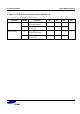
S3C84E5/C84E9/P84E9 USER’S MANUAL ERRATA ERRATA (VER 1.1) Samsung 8-bit CMOS S3C84E5/C84E9/P84E9 Microprocessor User’s Manual Document Number: 21.1-S3-C84E5/C84E9/P84E9-082005 Publication: August 2005 1. Features (PAGE 1-2) Built-in RESET circuit (LVR) • Low-Voltage reset (LVR value: 2.9 V) Operating Voltage Range • VLVR to 5.5V 2. Low Voltage Reset (PAGE 16-1) The on-chip Low Voltage Reset, features static reset when supply voltage is below a reference voltage value (Typical 2.9 V).
USER’S MANUAL ERRATA S3C84E5/C84E9/P84E9 3. Low Voltage Reset (PAGE 16-2) Watchdog RESET nRESET N.F Internal System RESET Longger than 1us VDD VIN VREF + Comparator - When the VDD level is lower than 2.9V N.F Longger than 1us VDD VREF BGR NOTES: 1. The target of voltage detection level is 2.9 V at VDD = 5 V 2. BGR is Band Gap voltage Reference Figure 16-1.
S3C84E5/C84E9/P84E9 USER’S MANUAL ERRATA 4. Table 17-3. D.C. Electrical Characteristics (PAGE 17-3) (TA = – 25 °C to + 85 °C, VDD = VLVR to 5.5 V) Parameter Input high voltage Input low voltage Symbol Conditions Min Typ. Max Unit – VDD V – 0.2VDD V VIH1 VDD = VLVR to 5.5 V All port and nRESET 0.8 VDD VIH2 VDD = VLVR (to 5.5 V XIN and XTIN VDD – 0.5 VIL1 VDD = VLVR to 5.5 V All ports and nRESET – VIL2 VDD = VLVR to 5.5 V XIN and XTIN 0.
USER’S MANUAL ERRATA S3C84E5/C84E9/P84E9 5. Table 17-3. D.C. Electrical Characteristics (PAGE 17-4) (TA = – 25 °C to + 85 °C, VDD = VLVR Parameter Pull-up resistor Symbol Conditions Min Typ.
S3C84E5/C84E9/P84E9 USER’S MANUAL ERRATA 6. Table 17-4. A.C. Electrical Characteristics (PAGE 17-5) (TA = – 25 °C to + 85 °C, VDD = VLVR to 5.5 V) 7. Table 17-5. Main Oscillator Frequency (PAGE 17-6) (TA = – 25 °C + 85 °C, VDD = VLVR to 5.5 V) Oscillator Main crystal or ceramic External clock (main system) Clock Circuit XIN XOUT C1 C2 XIN XOUT Test Condition Min Typ. Max Unit VDD = VLVR to 5.5 V 1 – 12 MHz VDD = VLVR to 5.5 V 1 – 12 8. Table 17-6.
USER’S MANUAL ERRATA S3C84E5/C84E9/P84E9 10. Table 17-8. Subsystem Oscillator (crystal) Stabilization Time (PAGE 17-7) (TA = 25 °C) Oscillator Normal mode Strong mode Test Condition Min Typ. Max Unit VDD = 4.5 V to 5.5 V – 800 1600 ms VDD = VLVR to 3.3 V – 10 s VDD = 4.5 V to 5.5 V – 400 800 ms VDD = VLVR to 3.3 V – 150 300 11. Table 17-9. Data Retention Supply Voltage in Stop Mode (PAGE 17-8) (TA = – 25 °C to + 85 °C, VDD = VLVR to 5.5 V) 12. Table 17-10.
S3C84E5/C84E9/P84E9 USER’S MANUAL ERRATA 13. Table 17-11. A/D Converter Electrical Characteristics (PAGE 17-11) (TA = – 25 °C to + 85 °C, VDD = VLVR to 5.5 V, VSS = 0 V) 14. Table 17-12. LVR (Low Voltage Reset) Circuit Characteristics (PAGE 17-12) (TA = 25 °C) Parameter Symbol Test Condition Min Typ Max Unit VLVR TA = 25 °C 2.6 2.9 3.2 V LVR voltage level 15. Figure 17-8.
S3C84E5/C84E9/P84E9 8-BIT CMOS MICROCONTROLLERS USER'S MANUAL Revision 1.
Important Notice The information in this publication has been carefully checked and is believed to be entirely accurate at the time of publication. Samsung assumes no responsibility, however, for possible errors or omissions, or for any consequences resulting from the use of the information contained herein.
Preface The S3C84E5/C84E9/P84E9 Microcontroller User's Manual is designed for application designers and programmers who are using the S3C84E5/C84E9/P84E9 microcontroller for application development. It is organized in two main parts: Part I Programming Model Part II Hardware Descriptions Part I contains software-related information to familiarize you with the microcontroller's architecture, programming model, instruction set, and interrupt structure.
Table of Contents Part I — Programming Model Chapter 1 Product Overview S3C8-SERIES Microcontrollers.............................................................................................................1-1 S3C84E5/C84E9/P84E9 Microcontroller ................................................................................................1-1 Features .............................................................................................................................................
Table of Contents Chapter 4 (Continued) Control Registers Overview .............................................................................................................................................4-1 Chapter 5 Interrupt Structure Overview .............................................................................................................................................5-1 Interrupt Types ..............................................................................................
Table of Contents (Continued) Part II Hardware Descriptions Chapter 7 Clock Circuit Overview .............................................................................................................................................7-1 System Clock Circuit...................................................................................................................7-1 Clock Status During Power-Down Modes .......................................................................................
Table of Contents Chapter 11 (Continued) 8-bit Timer A/B 8-Bit Timer A.......................................................................................................................................11-1 Overview .....................................................................................................................................11-1 Function Description....................................................................................................................
Table of Contents Chapter 15 (Continued) 8-bit Analog-to-Digital Converter Overview .............................................................................................................................................15-1 Function Description............................................................................................................................15-1 A/D Converter Control Register (ADCON).......................................................................................
List of Figures Figure Number Title Page Number 1-1 1-2 1-3 1-4 1-5 1-6 1-7 1-8 1-9 S3C84E5/C84E9/P84E9 Block Diagram ................................................................1-3 S3C84E5/C84E9/P84E9 Pin Assignment (44-pin QFP)...........................................1-4 S3C84E5/C84E9/P84E9 Pin Assignment (42-pin SDIP)..........................................1-5 Pin Circuit Type B (RESETB) ...............................................................................1-8 Pin Circuit Type C ....
List of Figures (Continued) Figure Number Title Page Number 5-1 5-2 5-3 5-4 5-5 5-6 5-7 5-8 5-9 S3C8-Series Interrupt Types .................................................................................5-2 S3C84E5/C84E9/P84E9 Interrupt Structure ...........................................................5-4 ROM Vector Address Area...................................................................................5-5 Interrupt Function Diagram ...........................................................
List of Figures (Concluded) Page Number Title Page Number 12-1 12-2 12-3 Timer 1(0,1) Control Register (T1CON0, T1CON1)...................................................12-4 Timer A, Timer 1(0,1) Pending Register (TINTPND) .................................................12-5 Timer 1(0,1) Functional Block Diagram ..................................................................12-6 13-1 13-2 13-3 13-4 13-5 13-6 13-7 13-8 13-9 UART Control Register (UARTCON) ..........................................
List of Tables Table Number Title Page Number 1-1 S3C84E5/C84E9/P84E9 Pin Descriptions..............................................................1-6 2-1 S3C84E5/C84E9/P84E9 Register Type Summary ..................................................2-3 4-1 4-2 4-3 Set 1 Registers ...................................................................................................4-1 Set 1, Bank 0 Registers .......................................................................................
List of Tables Table Number Title (Continued) Page Number 19-1 19-2 19-3 Descriptions of Pins Used to Read/Write the OTP ..................................................19-3 Comparison of S3P84E9 and S3C84E5/C84E9 Features.........................................19-3 Operating Mode Selection Criteria.........................................................................19-3 20-1 20-2 20-3 Power Selection Settings for TB84E5/84E9............................................................
List of Programming Tips Description Chapter 2: Page Number Address Spaces Using the Page Pointer for RAM clear (Page 0, Page 1)..........................................................................2-6 Setting the Register Pointers ................................................................................................................2-10 Using the RPs to Calculate the Sum of a Series of Registers ..................................................................
List of Register Descriptions Register Identifier ADCON BTCON CLKCON FLAGS IMR IPH IPL IPR IRQ OSCCON P0CONH P0CONL P1CONH P1CONL P2CONH P2CONL P2INT P2INTPND P3CONH P3CONL P4CONH P4CONL P4INT P4INTPND PP RP0 RP1 SPH SPL STPCON SYM T1CON0 T1CON1 TACON TBCON TINTPND UARTCON UARTPND WTCON Full Register Name Page Number A/D Converter Control Register F7H Set 1, Bank 0 .................................................4-5 Basic Timer Control Register H Set 1....................................................
List of Instruction Descriptions Instruction Mnemonic ADC ADD AND BAND BCP BITC BITR BITS BOR BTJRF BTJRT BXOR CALL CCF CLR COM CP CPIJE CPIJNE DA DA DEC DECW DI DIV DJNZ EI ENTER EXIT IDLE INC INCW IRET JP JR LD LD LDB Full Register Name Page Number Add with Carry ....................................................................................................6-14 Add....................................................................................................................6-15 Logical AND...
List of Instruction Descriptions (Continued) Instruction Mnemonic LDC/LDE LDC/LDE LDCD/LDED LDCI/LDEI LDCPD/LDEPD LDCPI/LDEPI LDW MULT NEXT NOP OR POP POPUD POPUI PUSH PUSHUD PUSHUI RCF RET RL RLC RR RRC SB0 SB1 SBC SCF SRA SRP/SRP0/SRP1 STOP SUB SWAP TCM TM WFI XOR xxii Full Register Name Page Number Load Memory ......................................................................................................6-52 Load Memory ..........................................................................
S3C84E5/C84E9/P84E9 1 PRODUCT OVERVIEW PRODUCT OVERVIEW S3C8-SERIES MICROCONTROLLERS Samsung's S3C8-series of 8-bit single-chip CMOS microcontrollers offers a fast and efficient CPU, a wide range of integrated peripherals, and various mask-programmable ROM sizes.
PRODUCT OVERVIEW S3C84E5/C84E9/P84E9 FEATURES CPU Watch timer • • Real-time and interval time measurement • Four-frequency outputs for buzzer sound SAM88RC CPU core Memory • • 528-bytes internal register file 16K/32Kbytes internal program memory (S3C84E5/C84E9:Mask ROM) (S3P84E9:OTP) Oscillation Sources • • • Main clock oscillator (Crystal, Ceramic) CPU clock divider (1/1, 1/2, 1/8, 1/16) 32,768Hz Sub oscillator for watch timer A/D Converter • • • Asynchronous UART • One Asynchronous UART •
S3C84E5/C84E9/P84E9 PRODUCT OVERVIEW BLOCK DIAGRAM P0.0~P0.7 P1.0~P1.5 Port 0 Port 1 Xin, XTin Xout, XTout OSC/nRESET nRESET 8-Bit Basic Timer P1.0/TAOUT P0.7/TACAP P0.6/TACK P4.3/TBPW M 8-Bit Timer/Counter A, B P1.2/T1OUT0 P1.1/T1CK0 P0.5/T1CAP0 P0.4/T1OUT1 P0.3/T1CK1 P0.2/T1CAP1 16-Bit Timer/Counter 10, 11 P1.5/TxD P1.4/RxD P1.3/BZOUT P2.0~P2.7/ INT0~INT7 Port 3 P3.0~P3.7/ ADC0~ADC7 Port 4 P4.0~P4.
PRODUCT OVERVIEW S3C84E5/C84E9/P84E9 44 43 42 41 40 39 38 37 36 35 34 P4.4 P0.2/T1CAP1 P0.3/T1CK1 P0.4/T1OUT1 P0.5/T1CAP0 P0.6/TACK P0.7/TACAP P1.0/TAOUT P1.1/T1CK0 P1.2/T1OUT0 P1.3/BZOUT PIN ASSIGNMENT S3C84E5 S3C84E9 S3P84E9 Top View (44-QFP) 12 13 14 15 16 17 18 19 20 21 22 1 2 3 4 5 6 7 8 9 10 11 33 32 31 30 29 28 27 26 25 24 23 P1.4/RXD P1.5/TXD P3.7/ADC7 P3.6/ADC6 P3.5/ADC5 P3.4/ADC4 P3.3/ADC3 P3.2/ADC2 P3.1/ADC1 P3.0/ADC0 AVss nRESET INT0/P2.0 INT1/P2.1 INT2/P2.2 INT3/P2.3 INT4/P2.4 INT5/P2.
S3C84E5/C84E9/P84E9 PRODUCT OVERVIEW PIN ASSIGNMENT TACAP/P0.7 TACK/P0.6 T1CAP0/P0.5 T1OUT1/P0.4 T1CK1/P0.3 T1CAP1/P0.2 XTout/P0.1 XTin/P0.0 TBPWM/P4.3 INT10/P4.2 VDD VSS Xout Xin TEST INT9/P4.1 INT8/P4.0 nRESET INT0/P2.0 INT1/P2.1 INT2/P2.2 1 2 3 4 5 6 7 8 9 10 11 12 13 14 15 16 17 18 19 20 21 S3C84E5 S3C84E9 S3P84E9 Top View (42-SDIP) 42 41 40 39 38 37 36 35 34 33 32 31 30 29 28 27 26 25 24 23 22 P1.0/TAOUT P1.1/T1CK0 P1.2/T1OUT0 P1.3/BZOUT P1.4/RXD P1.5/TXD P3.7/ADC7 P3.6/ADC6 P3.5/ADC5 P3.
PRODUCT OVERVIEW S3C84E5/C84E9/P84E9 PIN DESCRIPTIONS Table 1-1. S3C84E5/C84E9/P84E9 Pin Descriptions Pin Name Pin Type P0.0–P0.7 I/O P1.0–P1.5 Pin Description Circuit Type Pin Number Share Pins Bit programmable port; input or output mode selected by software; input or push-pull output. Software assignable pull-up resistor. Alternately, can be used as I/O for Timer A, Timer 1(0,1). P0.0 and P0.
S3C84E5/C84E9/P84E9 PRODUCT OVERVIEW Table 1-1. S3C84E5/C84E9/P84E9 Pin Descriptions (Continued) Pin Name Pin Type Pin Description Circuit Type Pin Number Share Pins INT0–INT10 I Input pins for external interrupt. Alternatively used as general-purpose digital input/output port 2,4. D-1 13-20, 4 P2.0–P2.7 10-11 P4.0–P4.2 (19-26) (10,16-17) ADC0–ADC7 I Analog input pins for A/D converter module. Alternatively used as general-purpose digital input/output port 3. E 24-31 (29-36) P3.0–P3.
PRODUCT OVERVIEW S3C84E5/C84E9/P84E9 PIN CIRCUITS VDD Pull-Up Resistor In Schmitt Trigger Figure 1-4. Pin Circuit Type B (nRESET) VDD Data P-Channel Out Output Disable N-Channel Figure 1-5.
S3C84E5/C84E9/P84E9 PRODUCT OVERVIEW VDD Pull-up Enable Data Output Disable Pin Circuit Type C I/O Figure 1-6. Pin Circuit Type D (P0.2-P0.7, P1, P4.3–P4.5) VDD VDD Data Pin Circuit Type C Output Disable Ext.INT Pull-up Enable I/O Noise Filter Input Normal Figure 1-7. Pin Circuit Type D-1 (P2, and P4.0–P4.
PRODUCT OVERVIEW S3C84E5/C84E9/P84E9 VDD Pull-up Resistor (Typical Value: 47kΩ) Pull-up Enable VDD Data In/Out Output DIsable Normal Input Analog Input Figure 1-8. Pin Circuit Type E (P3) VDD Pull-up enable VDD P-CH Output Data Output Disable (Input Mode) I/O N-CH Digital Input Alternative I/O Enable XTin, XTout Oscillation circuit Figure 1-9. Pin Circuit Type F (P0.0, P0.
S3C84E5/C84E9/P84E9 2 ADDRESS SPACES ADDRESS SPACES OVERVIEW The S3C84E5/C84E9/P84E9 microcontroller has two types of address space: — Internal program memory (ROM) — Internal register file (RAM) A 16-bit address bus supports program memory operations. A separate 8-bit register bus carries addresses and data between the CPU and the register file. The S3C84E5/C84E9/P84E9 has an internal 16/32-Kbyte mask-programmable ROM / 32-Kbyte OTP ROM and 528byte RAM.
ADDRESS SPACES S3C84E5/C84E9/P84E9 PROGRAM MEMORY (ROM) Program memory (ROM) stores program codes or table data. The S3C84E5/84E9 has 16Kbytes and 32Kbytes of internal mask programmable program memory. The program memory address range is therefore 0H–3FFFH and 0H7FFFH (see Figure 2-1). The first 256 bytes of the ROM (0H-0FFH) are reserved for interrupt vector addresses. Unused locations in this address range can be used as normal program memory.
S3C84E5/C84E9/P84E9 ADDRESS SPACES REGISTER ARCHITECTURE In the S3C84E5/C84E9/P84E9 implementation, the upper 64-byte area of register files is expanded two 64-byte areas, called set 1 and set 2. The upper 32-byte area of set 1 is further expanded two 32-byte register banks (bank 0 and bank 1), and the lower 32-byte area is a single 32-byte common area. set 2 is logically expanded 2 separately addressable register pages, page 0–page 1.
ADDRESS SPACES S3C84E5/C84E9/P84E9 Set1 Bank 1 FFH 32 Bytes Page01 Page FFH FFH Bank 0 System and Peripheral Control Registers (Register Addressing Mode) Set 2 General-Purpose Data Registers Page 0 Page 0 (Indirect Register,Page Indexed 0 Mode, and StackPage Operations) 0 E0H E0H 64 Bytes DFH D0H CFH Page Page00 System and Peripheral Control Registers (Register Addressing Mode) Page 0 C0H BFH General Purpose Register (Register Addressing Mode) Page 0 Page 0 C0H Prime Data Registers 192 Byte
S3C84E5/C84E9/P84E9 ADDRESS SPACES REGISTER PAGE POINTER (PP) The S3C8-series architecture supports the logical expansion of the physical 512-byte internal register file (using an 8-bit data bus) into as many as 2 separately addressable register pages. Page addressing is controlled by the register page pointer (PP, DFH). In the S3C84E5/C84E9/P84E9 microcontroller, a paged register file expansion is implemented for data registers, and the register page pointer must be changed to address other pages.
ADDRESS SPACES S3C84E5/C84E9/P84E9 F PROGRAMMING TIP — Using the Page Pointer for RAM clear (Page 0, Page 1) RAMCL0: RAMCL1: 2-6 ; Destination ← 0, Source ← 0 LD PP,#00H SRP #0C0H LD R0,#0FFH CLR @R0 DJNZ R0,RAMCL0 CLR @R0 ; R0 = 00H LD PP,#10H ; Destination ← 1, Source ← 0 LD R0,#0FFH ; Page 1 RAM clear starts CLR @R0 DJNZ R0,RAMCL1 CLR @R0 ; Page 0 RAM clear starts ; R0 = 00H
S3C84E5/C84E9/P84E9 ADDRESS SPACES REGISTER SET 1 The term set 1 refers to the upper 64 bytes of the register file, locations C0H–FFH. The upper 32-byte area of this 64-byte space (E0H–FFH) is expanded two 32-byte register banks, bank 0 and bank 1. The set register bank instructions, SB0 or SB1, are used to address one bank or the other. A hardware reset operation always selects bank 0 addressing.
ADDRESS SPACES S3C84E5/C84E9/P84E9 PRIME REGISTER SPACE The lower 192 bytes (00H–BFH) of the S3C84E5/C84E9/P84E9's two 256-byte register pages is called prime register area. Prime registers can be accessed using any of the seven addressing modes (see Chapter 3, "Addressing Modes.") The prime register area on page 0 is immediately addressable following a reset. In order to address prime registers on pages 0, or 1 you must set the register page pointer (PP) to the appropriate source and destination values.
S3C84E5/C84E9/P84E9 ADDRESS SPACES WORKING REGISTERS Instructions can access specific 8-bit registers or 16-bit register pairs using either 4-bit or 8-bit address fields. When 4-bit working register addressing is used, the 256-byte register file can be seen by the programmer as one that consists of 32 8-byte register groups or "slices." Each slice comprises of eight 8-bit registers.
ADDRESS SPACES S3C84E5/C84E9/P84E9 USING THE REGISTER POINTERS Register pointers RP0 and RP1, mapped to addresses D6H and D7H in set 1, are used to select two movable 8-byte working register slices in the register file. After a reset, RP# point to the working register common area: RP0 points to addresses C0H–C7H, and RP1 points to addresses C8H–CFH. To change a register pointer value, you load a new value to RP0 and or RP1 using an SRP or LD instruction. (see Figures 2-6 and 2-7).
S3C84E5/C84E9/P84E9 ADDRESS SPACES F7H (R7) 8-Byte Slice F0H (R0) Register File Contains 32 8-Byte Slices 1 1 1 1 0 X X X 16-byte Noncontiguous working register block RP0 7H (R15) 0 0 0 0 0 X X X 8-Byte Slice 0H (R8) RP1 Figure 2-7. Non-Contiguous 16-Byte Working Register Block F PROGRAMMING TIP — Using the RPs to Calculate the Sum of a Series of Registers Calculate the sum of registers 80H–85H using the register pointer.
ADDRESS SPACES S3C84E5/C84E9/P84E9 REGISTER ADDRESSING The S3C8-series register architecture provides an efficient method of working register addressing that takes full advantage of shorter instruction formats to reduce execution time. With Register (R) addressing mode, in which the operand value is the content of a specific register or register pair, you can access any location in the register file except for set 2.
S3C84E5/C84E9/P84E9 ADDRESS SPACES Special-Purpose Registers Bank 1 General-Purpose Register Bank 0 FFH FFH Control Registers Set 2 E0H System Registers D0H CFH C0H BFH C0H RP1 Register Pointers RP0 Each register pointer (RP) can independently point to one of the 24 8-byte "slices" of the register file (other than set 2). After a reset, RP0 points to locations C0H-C7H and RP1 to locations C8H-CFH (that is, to the common working register area).
ADDRESS SPACES S3C84E5/C84E9/P84E9 COMMON WORKING REGISTER AREA (C0H–CFH) After a reset, register pointers RP0 and RP1 automatically select two 8-byte register slices in set 1, locations C0H– CFH, as the active 16-byte working register block: RP0 → C0H–C7H RP1 → C8H–CFH This 16-byte address range is called common area. That is, locations in this area can be used as working registers by operations that address any location on any page in the register file.
S3C84E5/C84E9/P84E9 ADDRESS SPACES F PROGRAMMING TIP — Addressing the Common Working Register Area As the following examples show, you should access working registers in the common area, locations C0H–CFH, using working register addressing mode only. Examples 1: 1.
ADDRESS SPACES S3C84E5/C84E9/P84E9 RP0 RP1 Selects RP0 or RP1 Address OPCODE 4-bit address provides three low-order bits Register pointer provides five high-order bits Together they create an 8-bit register address Figure 2-11. 4-Bit Working Register Addressing RP0 0 1 1 1 0 RP1 0 0 0 0 1 1 1 1 0 0 0 Selects RP0 0 1 1 1 0 1 1 0 Register address (76H) R6 OPCODE 0 1 1 0 1 1 1 0 Instruction 'INC R6' Figure 2-12.
S3C84E5/C84E9/P84E9 ADDRESS SPACES 8-BIT WORKING REGISTER ADDRESSING You can also use 8-bit working register addressing to access registers in a selected working register area. To initiate 8-bit working register addressing, the upper four bits of the instruction address must contain the value "1100B." This 4-bit value (1100B) indicates that the remaining four bits have the same effect as 4-bit working register addressing.
ADDRESS SPACES S3C84E5/C84E9/P84E9 RP0 0 1 1 0 0 RP1 0 0 0 1 0 1 0 1 0 0 0 1 0 1 0 1 0 1 1 Selects RP1 R11 1 1 0 0 1 0 1 1 8-bit address form instruction 'LD R11, R2' Specifies working register addressing Figure 2-14.
S3C84E5/C84E9/P84E9 ADDRESS SPACES SYSTEM AND USER STACK The S3C8-series microcontrollers use the system stack for data storage, subroutine calls and returns. The PUSH and POP instructions are used to control system stack operations. The S3C84E5/C84E9/P84E architecture supports stack operations in the internal register file. Stack Operations Return addresses for procedure calls, interrupts, and data are stored on the stack.
ADDRESS SPACES S3C84E5/C84E9/P84E9 F PROGRAMMING TIP — Standard Stack Operations Using PUSH and POP The following example shows you how to perform stack operations in the internal register file using PUSH and POP instructions: LD SPL,#0FFH ; SPL ← FFH ; (Normally, the SPL is set to 0FFH by the initialization ; routine) • • • PUSH PP ; Stack address 0FEH ← PP PUSH RP0 ; Stack address 0FDH ← RP0 PUSH RP1 ; Stack address 0FCH ← RP1 PUSH R3 ; Stack address 0FBH ← R3 • • • 2-20 POP R3 ; R3
S3C84E5/C84E9/P84E9 3 ADDRESSING MODES ADDRESSING MODES OVERVIEW Instructions that are stored in program memory are fetched for execution using the program counter. Instructions indicate the operation to be performed and the data to be operated on. Addressing mode is the method used to determine the location of the data operand. The operands specified in SAM88RC instructions may be condition codes, immediate data, or a location in the register file, program memory, or data memory.
ADDRESSING MODES S3C84E5/C84E9/P84E9 REGISTER ADDRESSING MODE (R) In Register addressing mode (R), the operand value is the content of a specified register or register pair (see Figure 3-1). Working register addressing differs from Register addressing in that it uses a register pointer to specify an 8-byte working register space in the register file and an 8-bit register within that space (see Figure 3-2).
S3C84E5/C84E9/P84E9 ADDRESSING MODES INDIRECT REGISTER ADDRESSING MODE (IR) In Indirect Register (IR) addressing mode, the content of the specified register or register pair is the address of the operand. Depending on the instruction used, the actual address may point to a register in the register file, to program memory (ROM), or to an external memory space (see Figures 3-3 through 3-6). You can use any 8-bit register to indirectly address another register.
ADDRESSING MODES S3C84E5/C84E9/P84E9 INDIRECT REGISTER ADDRESSING MODE (Continued) Register File Program Memory Example Instruction References Program Memory REGISTER dst OPCODE PAIR Points to Register Pair Program Memory Sample Instructions: CALL JP @RR2 @RR2 Value used in Instruction OPERAND Figure 3-4.
S3C84E5/C84E9/P84E9 ADDRESSING MODES INDIRECT REGISTER ADDRESSING MODE (Continued) Register File MSB Points to RP0 or RP1 Program Memory 4-bit Working Register Address dst src OPCODE RP0 or RP1 ~ ~ 3 LSBs Point to the Working Register (1 of 8) ADDRESS ~ Sample Instruction: OR R3, @R6 Value used in Instruction Selected RP points to start fo working register block ~ OPERAND Figure 3-5.
ADDRESSING MODES S3C84E5/C84E9/P84E9 INDIRECT REGISTER ADDRESSING MODE (Continued) Register File MSB Points to RP0 or RP1 RP0 or RP1 Selected RP points to start of working register block Program Memory 4-bit Working Register Address dst Example Instruction References either Program Memory or Data Memory src OPCODE Next 2-bit Point to Working Register Pair (1 of 4) LSB Selects Value used in Instruction Register Pair Program Memory or Data Memory 16-Bit address points to program memory or data mem
S3C84E5/C84E9/P84E9 ADDRESSING MODES INDEXED ADDRESSING MODE (X) Indexed (X) addressing mode adds an offset value to a base address during instruction execution in order to calculate the effective operand address (see Figure 3-7). You can use Indexed addressing mode to access locations in the internal register file or in external memory. Please note, however, that you cannot access locations C0H–FFH in set 1 using indexed addressing mode.
ADDRESSING MODES S3C84E5/C84E9/P84E9 INDEXED ADDRESSING MODE (Continued) Register File MSB Points to RP0 or RP1 RP0 or RP1 ~ ~ Program Memory OFFSET 4-bit Working Register Address dst/src Selected RP points to start of working register block NEXT 2 Bits x OPCODE Point to Working Register Pair (1 of 4) LSB Selects + 8-Bits Register Pair Program Memory or Data Memory 16-Bit address added to offset 16-Bits 16-Bits OPERAND Value used in Instruction Sample Instructions: LDC R4, #04H[RR2] L
S3C84E5/C84E9/P84E9 ADDRESSING MODES INDEXED ADDRESSING MODE (Continued) Register File MSB Points to RP0 or RP1 RP0 or RP1 Program Memory 4-bit Working Register Address ~ OFFSET OFFSET dst/src src OPCODE ~ Selected RP points to start of working register block NEXT 2 Bits Point to Working Register Pair LSB Selects + 16-Bits Register Pair Program Memory or Data Memory 16-Bit address added to offset 16-Bits 16-Bits OPERAND Value used in Instruction Sample Instructions: LDC R4, #1000H[RR2]
ADDRESSING MODES S3C84E5/C84E9/P84E9 DIRECT ADDRESS MODE (DA) In Direct Address (DA) mode, the instruction provides the operand's 16-bit memory address. Jump (JP) and Call (CALL) instructions use this addressing mode to specify the 16-bit destination address that is loaded into the PC whenever a JP or CALL instruction is executed.
S3C84E5/C84E9/P84E9 ADDRESSING MODES DIRECT ADDRESS MODE (Continued) Program Memory Next OPCODE Memory Address Used Upper Address Byte Lower Address Byte OPCODE Sample Instructions: JP CALL C,JOB1 DISPLAY ; ; Where JOB1 is a 16-bit immediate address Where DISPLAY is a 16-bit immediate address Figure 3-11.
ADDRESSING MODES S3C84E5/C84E9/P84E9 INDIRECT ADDRESS MODE (IA) In Indirect Address (IA) mode, the instruction specifies an address located in the lowest 256 bytes of the program memory. The selected pair of memory locations contains the actual address of the next instruction to be executed. Only the CALL instruction can use the Indirect Address mode.
S3C84E5/C84E9/P84E9 ADDRESSING MODES RELATIVE ADDRESS MODE (RA) In Relative Address (RA) mode, a twos-complement signed displacement between – 128 and + 127 is specified in the instruction. The displacement value is then added to the current PC value. The result is the address of the next instruction to be executed. Before this addition occurs, the PC contains the address of the instruction immediately following the current instruction.
ADDRESSING MODES S3C84E5/C84E9/P84E9 IMMEDIATE MODE (IM) In Immediate (IM) addressing mode, the operand value used in the instruction is the value supplied in the operand field itself. The operand may be one byte or one word in length, depending on the instruction used. Immediate addressing mode is useful for loading constant values into registers. Program Memory OPERAND OPCODE (The Operand value is in the instruction) Sample Instruction: LD R0,#0AAH Figure 3-14.
S3C84E5/C84E9/P84E9 4 CONTROL REGISTER CONTROL REGISTERS OVERVIEW Control register descriptions are arranged in alphabetical order according to register mnemonic. More detailed information about control registers is presented in the context of the specific peripheral hardware descriptions in Part II of this manual. The locations and read/write characteristics of all mapped registers in the S3C84E5/C84E9/P84E9 register file are listed in Table 4-1.
CONTROL REGISTERS S3C84E5/C84E9/P84E9 Table 4-2.
S3C84E5/C84E9/P84E9 CONTROL REGISTER Table 4-3.
CONTROL REGISTERS S3C84E5/C84E9/P84E9 Name of individual bit or related bits Bit number(s) that is/are appended to the register name for bit addressing Register ID Register name Register location Register address in the internal register file (hexadecimal) FLAGS - System Flags Register Bit Identifier RESET Value Read/Write Bit Addressing .7 .6 D5H .5 .4 x x x x R/W R/W R/W R/W Register addressing mode only Set 1 .3 .2 .1 .0 x R/W x R/W 0 R 0 R/W Mode .7 Carry Flag (C) .
S3C84E5/C84E9/P84E9 CONTROL REGISTER ADCON — A/D Converter Control Register F7H Set 1, Bank 0 Bit Identifier .7 .6 .5 .4 .3 .2 .1 .0 Reset Value 0 0 0 0 0 0 0 0 Read/Write – R/W R/W R/W R R/W R/W R/W Addressing Mode Register addressing mode only .7 Not used for the S3C84E5/C84E9/P84E9 (must keep always 0) .6–.4 A/D Input Pin Selection Bits .3 .2–.1 .
CONTROL REGISTERS S3C84E5/C84E9/P84E9 BTCON — Basic Timer Control Register D3H Set 1 Bit Identifier .7 .6 .5 .4 .3 .2 .1 .0 Reset Value 0 0 0 0 0 0 0 0 Read/Write R/W R/W R/W R/W R/W R/W R/W R/W Addressing Mode Register addressing mode only .7–.4 Watchdog Timer Function Disable Code (for System Reset) 1 0 1 0 Other Values .3–.2 .1 .
S3C84E5/C84E9/P84E9 CONTROL REGISTER CLKCON — System Clock Control Register D4H Set 1 Bit Identifier .7 .6 .5 .4 .3 .2 .1 .0 Reset Value 0 0 0 0 0 0 0 0 Read/Write – – – R/W R/W – – – Addressing Mode Register addressing mode only .7–.5 Not used for the S3C84E5/C84E9/P84E9 (must keep always 0) .4–.3 CPU Clock (System Clock) Selection Bits (note) .2–.
CONTROL REGISTERS S3C84E5/C84E9/P84E9 FLAGS — System Flags Register D5H Set 1 Bit Identifier .7 .6 .5 .4 .3 .2 .1 .0 Reset Value x x x x x x 0 0 Read/Write R/W R/W R/W R/W R/W R/W R R/W Addressing Mode Register addressing mode only .7 Carry Flag (C) .6 .5 .4 .3 .2 .1 .
S3C84E5/C84E9/P84E9 CONTROL REGISTER IMR — Interrupt Mask Register DDH Set 1 Bit Identifier .7 .6 .5 .4 .3 .2 .1 .0 Reset Value x x x x x x x x Read/Write R/W R/W R/W R/W R/W R/W R/W R/W Addressing Mode Register addressing mode only .7 Interrupt Level 7 (IRQ7) Enable Bit .6 .5 .4 .3 .2 .1 .
CONTROL REGISTERS S3C84E5/C84E9/P84E9 IPH — Instruction Pointer (High Byte) DAH Set 1 Bit Identifier .7 .6 .5 .4 .3 .2 .1 .0 Reset Value x x x x x x x x Read/Write R/W R/W R/W R/W R/W R/W R/W R/W Addressing Mode Register addressing mode only .7–.0 Instruction Pointer Address (High Byte) The high-byte instruction pointer value is the upper eight bits of the 16-bit instruction pointer address (IP15–IP8). The lower byte of the IP address is located in the IPL register (DBH).
S3C84E5/C84E9/P84E9 CONTROL REGISTER IPR — Interrupt Priority Register FFH Set 1, Bank 0 Bit Identifier .7 .6 .5 .4 .3 .2 .1 .0 Reset Value x x x x x x x x Read/Write R/W R/W R/W R/W R/W R/W R/W R/W Addressing Mode Register addressing mode only .7, .4, and .1 Priority Control Bits for Interrupt Groups A, B, and C .6 .5 .3 .2 .
CONTROL REGISTERS S3C84E5/C84E9/P84E9 IRQ — Interrupt Request Register DCH Set 1 Bit Identifier .7 .6 .5 .4 .3 .2 .1 .0 Reset Value 0 0 0 0 0 0 0 0 Read/Write R R R R R R R R Addressing Mode Register addressing mode only .7 Interrupt Level 7 (IRQ7) Request Pending Bit .6 .5 .4 .3 .2 .1 .
S3C84E5/C84E9/P84E9 CONTROL REGISTER OSCCON — Oscillator Control Register FBH Set 1, Bank 0 Bit Identifier .7 .6 .5 .4 .3 .2 .1 .0 Reset Value 0 0 0 0 0 0 0 0 Read/Write – – – R/W R/W R/W – R/W Addressing Mode Register addressing mode only .7–.5 Not used for the S3C84E5/C84E9/P84E9 (must keep always 0) .4 Sub-system Oscillator Driving Ability Control Bit .3 .
CONTROL REGISTERS S3C84E5/C84E9/P84E9 P0CONH — Port 0 Control Register (High Byte) E6H Set 1, Bank 0 Bit Identifier .7 .6 .5 .4 .3 .2 .1 .0 Reset Value 0 0 0 0 0 0 0 0 Read/Write R/W R/W R/W R/W R/W R/W R/W R/W Addressing Mode Register addressing mode only .7–.6 P0.7/TACAP Configuration Bits .5–.4 .3–.2 .1–.0 4-14 0 0 Input mode with pull-up; TACAP input 0 1 Input mode; TACAP input 1 X Push-pull output mode P0.
S3C84E5/C84E9/P84E9 CONTROL REGISTER P0CONL — Port 0 Control Register (Low Byte) E7H Set 1, Bank 0 Bit Identifier .7 .6 .5 .4 .3 .2 1 .0 Reset Value 0 0 0 0 1 1 1 1 Read/Write R/W R/W R/W R/W R/W R/W R/W R/W Addressing Mode Register addressing mode only .7–.6 P0.3/T1CK1 Configuration Bits .5–.4 .3–.2 .1–.0 0 0 Input mode with pull-up; T1CK1 input 0 1 Input mode; T1CK1 input 1 X Push-pull output mode P0.
CONTROL REGISTERS S3C84E5/C84E9/P84E9 P1CONH — Port 1 Control Register (High Byte) E8H Set 1, Bank 0 Bit Identifier .7 .6 .5 .4 .3 .2 .1 .0 Reset Value 0 0 0 0 0 0 0 0 Read/Write – – – – R/W R/W R/W R/W Addressing Mode Register addressing mode only .7–.4 Not used for the S3C84E5/C84E9/P84E9 (must keep always 0) .3–.2 P1.5/TXD Configuration Bits .1–.
S3C84E5/C84E9/P84E9 CONTROL REGISTER P1CONL — Port 1 Control Register (Low Byte) E9H Set 1, Bank 0 Bit Identifier .7 .6 .5 .4 .3 .2 .1 .0 Reset Value 0 0 0 0 0 0 0 0 Read/Write R/W R/W R/W R/W R/W R/W R/W R/W Addressing Mode Register addressing mode only .7–.6 P1.3/BZOUT Configuration Bits .5–.4 .3–.2 .1–.0 0 0 Input mode with pull-up 0 1 Input mode 1 0 Push-pull output mode 1 1 Alternative function mode: BZOUT output P1.
CONTROL REGISTERS S3C84E5/C84E9/P84E9 P2CONH — Port 2 Control Register (High Byte) EAH Set 1, Bank 0 Bit Identifier .7 .6 .5 .4 .3 .2 .1 .0 Reset Value 0 0 0 0 0 0 0 0 Read/Write R/W R/W R/W R/W R/W R/W R/W R/W Addressing Mode Register addressing mode only .7–.6 P2.7/INT7 .5-.4 .3–.2 .1–.
S3C84E5/C84E9/P84E9 CONTROL REGISTER P2CONL — Port 2 Control Register (Low Byte) EBH Set 1, Bank 0 Bit Identifier .7 .6 .5 .4 .3 .2 .1 .0 Reset Value 0 0 0 0 0 0 0 0 Read/Write R/W R/W R/W R/W R/W R/W R/W R/W Addressing Mode Register addressing mode only .7–.6 P2.3/INT3 .5–.4 .3–.2 .1–.
CONTROL REGISTERS S3C84E5/C84E9/P84E9 P2INT — Port 2 Interrupt Control Register ECH Set 1, Bank 0 Bit Identifier .7 .6 .5 .4 .3 .2 .1 .0 Reset Value 0 0 0 0 0 0 0 0 Read/Write R/W R/W R/W R/W R/W R/W R/W R/W Addressing Mode Register addressing mode only .7 P2.7 External Interrupt (INT7) Enable Bit .6 .5 .4 .3 .2 .1 .0 4-20 0 Disable interrupt 1 Enable interrupt P2.6 External Interrupt (INT6) Enable Bit 0 Disable interrupt 1 Enable interrupt P2.
S3C84E5/C84E9/P84E9 CONTROL REGISTER P2INTPND — Port 2 Interrupt Pending Register EDH Set 1, Bank 0 Bit Identifier .7 .6 .5 .4 .3 .2 .1 .0 Reset Value 0 0 0 0 0 0 0 0 Read/Write R/W R/W R/W R/W R/W R/W R/W R/W Addressing Mode Register addressing mode only .7 P2.7/PND7 Interrupt Pending Bit .6 .5 .4 .3 .2 .1 .0 0 Interrupt request is not pending, pending bit clear when write 0 1 Interrupt request is pending P2.
CONTROL REGISTERS S3C84E5/C84E9/P84E9 P3CONH — Port 3 Control Register (High Byte) EEH Set 1, Bank 0 Bit Identifier .7 .6 .5 .4 .3 .2 .1 .0 Reset Value 0 0 0 0 0 0 0 0 Read/Write R/W R/W R/W R/W R/W R/W R/W R/W Addressing Mode Register addressing mode only .7–.6 P3.7/ADC7 .5–.4 .3–.2 .1–.0 4-22 0 0 Input mode with pull-up 0 1 Input mode 1 0 Push-pull output mode 1 1 Alternative function mode: ADC7 input P3.
S3C84E5/C84E9/P84E9 CONTROL REGISTER P3CONL — Port 3 Control Register (Low Byte) EFH Set 1, Bank 0 Bit Identifier .7 .6 .5 .4 .3 .2 .1 .0 Reset Value 0 0 0 0 0 0 0 0 Read/Write R/W R/W R/W R/W R/W R/W R/W R/W Addressing Mode Register addressing mode only .7–.6 P3.3/ADC3 .5–.4 .3–.3 .1–.0 0 0 Input mode with pull-up 0 1 Input mode 1 0 Push-pull output mode 1 1 Alternative function mode: ADC3 input P3.
CONTROL REGISTERS S3C84E5/C84E9/P84E9 P4CONH — Port 4 Control Register (High Byte) F0H Set 1, Bank 0 Bit Identifier .7 .6 .5 .4 .3 .2 .1 .0 Reset Value 0 0 0 0 0 0 0 0 Read/Write – – – – R/W R/W R/W R/W Addressing Mode Register addressing mode only .7–.4 Not used for the S3C84E5/C84E9/P84E9 (must keep always 0) .3–.2 P4.5 .1–.
S3C84E5/C84E9/P84E9 CONTROL REGISTER P4CONL — Port 4 Control Register (Low Byte) F1H Set 1, Bank 0 Bit Identifier .7 .6 .5 .4 .3 .2 .1 .0 Reset Value 0 0 0 0 0 0 0 0 Read/Write R/W R/W R/W R/W R/W R/W R/W R/W Addressing Mode Register addressing mode only .7–.6 P4.3/TBPWM .5–.4 .3–.2 .1–.0 0 0 Input mode with pull-up 0 1 Input mode 1 0 Push-pull output mode 1 1 Alternative function mode: TBPWM output P4.
CONTROL REGISTERS S3C84E5/C84E9/P84E9 P4INT — Port 4 Interrupt Control Register F2H Set 1, Bank 0 Bit Identifier .7 .6 .5 .4 .3 .2 .1 .0 Reset Value 0 0 0 0 0 0 0 0 Read/Write – – – – – R/W R/W R/W Addressing Mode Register addressing mode only .7–.3 Not used for the S3C84E5/C84E9/P84E9 (must keep always 0) .2 P4.2 External Interrupt (INT10) Enable Bit .1 .0 4-26 0 Disable interrupt 1 Enable interrupt P4.
S3C84E5/C84E9/P84E9 CONTROL REGISTER P4INTPND — Port 4 Interrupt Pending Register F3H Set 1, Bank 0 Bit Identifier .7 .6 .5 .4 .3 .2 .1 .0 Reset Value 0 0 0 0 0 0 0 0 Read/Write – – – – – R/W R/W R/W Addressing Mode Register addressing mode only .7–.3 Not used for the S3C84E5/C84E9/P84E9 (must keep always 0) .2 P4.2/PND10 Interrupt Pending Bit .1 .0 0 Interrupt request is not pending, pending bit clear when write 0 1 Interrupt request is pending P4.
CONTROL REGISTERS S3C84E5/C84E9/P84E9 PP — Register Page Pointer DFH Set 1 Bit Identifier .7 .6 .5 .4 .3 .2 .1 .0 Reset Value 0 0 0 0 0 0 0 0 Read/Write R/W R/W R/W R/W R/W R/W R/W R/W Addressing Mode Register addressing mode only .7–.4 Destination Register Page Selection Bits 0 0 0 0 Destination: page 0 0 0 0 1 Destination: page 1 Other values .3–.
S3C84E5/C84E9/P84E9 CONTROL REGISTER RP0 — Register Pointer 0 D6H Set 1 Bit Identifier .7 .6 .5 .4 .3 .2 .1 .0 Reset Value 1 1 0 0 0 – – – Read/Write R/W R/W R/W R/W R/W – – – Addressing Mode Register addressing only .7–.3 Register Pointer 0 Address Value Register pointer 0 can independently point to one of the 256-byte working register areas in the register file.
CONTROL REGISTERS S3C84E5/C84E9/P84E9 SPH — Stack Pointer (High Byte) D8H Set 1 Bit Identifier .7 .6 .5 .4 .3 .2 .1 .0 Reset Value x x x x x x x x Read/Write R/W R/W R/W R/W R/W R/W R/W R/W Addressing Mode Register addressing mode only .7–.0 Stack Pointer Address (High Byte) The high-byte stack pointer value is the upper eight bits of the 16-bit stack pointer address (SP15–SP8). The lower byte of the stack pointer value is located in register SPL (D9H).
S3C84E5/C84E9/P84E9 CONTROL REGISTER STPCON — Stop Control Register E5H Set 1, Bank 0 Bit Identifier .7 .6 .5 .4 .3 .2 .1 .0 Reset Value 0 0 0 0 0 0 0 0 Read/Write R/W R/W R/W R/W R/W R/W R/W R/W Addressing Mode Register addressing mode only .7–.0 STOP Control Bits NOTE: 10100101 Enable stop instruction Other values Disable stop instruction Before execute the STOP instruction, You must set this STPCON register as “10100101b”.
CONTROL REGISTERS S3C84E5/C84E9/P84E9 SYM — System Mode Register DEH Set 1 Bit Identifier .7 .6 .5 .4 .3 .2 .1 .0 Reset Value 0 0 0 x x x 0 0 Read/Write – – – R/W R/W R/W R/W R/W Addressing Mode Register addressing mode only .7–.5 Not used, But you must keep always 0 .4–.2 Fast Interrupt Level Selection Bits .1 .
S3C84E5/C84E9/P84E9 CONTROL REGISTER T1CON0 — Timer 1(0) Control Register E8H Set 1, Bank 1 Bit Identifier .7 .6 .5 .4 .3 .2 .1 .0 Reset Value 0 0 0 0 0 0 0 0 Read/Write R/W R/W R/W R/W R/W R/W R/W R/W Addressing Mode Register addressing mode only .7–.5 Timer 1(0) Input Clock Selection Bits .4–.3 .2 .1 .
CONTROL REGISTERS S3C84E5/C84E9/P84E9 T1CON1 — Timer 1(1) Control Register E9H Set 1, Bank 1 Bit Identifier .7 .6 .5 .4 .3 .2 .1 .0 Reset Value 0 0 0 0 0 0 0 0 Read/Write R/W R/W R/W R/W R/W R/W R/W R/W Addressing Mode Register addressing mode only .7–.5 Timer 1(1) Input Clock Selection Bits .4–.3 .2 .1 .
S3C84E5/C84E9/P84E9 CONTROL REGISTER TACON — Timer A Control Register E1H Set 1, Bank 1 Bit Identifier .7 .6 .5 .4 .3 .2 .1 .0 Reset Value 0 0 0 0 0 0 0 0 Read/Write R/W R/W R/W R/W R/W R/W R/W R/W Addressing Mode Register addressing mode only .7–.6 Timer A Input Clock Selection Bits .5–.4 .3 .2 .1 .
CONTROL REGISTERS S3C84E5/C84E9/P84E9 TBCON — Timer B Control Register D0H Set 1 Bit Identifier .7 .6 .5 .4 .3 .2 .1 .0 Reset Value 0 0 0 0 0 0 0 0 Read/Write R/W R/W R/W R/W R/W R/W R/W R/W Addressing Mode Register addressing mode only .7–.6 Timer B Input Clock Selection Bits .5–.4 .3 .2 .1 .
S3C84E5/C84E9/P84E9 CONTROL REGISTER TINTPND — Timer A, Timer 1 Interrupt Pending Register E0H Set 1, Bank 1 Bit Identifier .7 .6 .5 .4 .3 .2 .1 .0 Reset Value 0 0 0 0 0 0 0 0 Read/Write – – R/W R/W R/W R/W R/W R/W Addressing Mode Register addressing mode only .7–.6 Not used for the S3C84E5/C84E9/P84E9 (must keep always 0) .5 Timer 1(1) Overflow Interrupt Pending Bit .4 .3 .2 .1 .
CONTROL REGISTERS S3C84E5/C84E9/P84E9 UARTCON — UART Control Register F6H Set 1, Bank 0 Bit Identifier .7 .6 .5 .4 .3 .2 .1 .0 Reset Value 0 0 0 0 0 0 0 0 Read/Write R/W R/W R/W R/W R/W R/W R/W R/W .7–.6 .5 .
S3C84E5/C84E9/P84E9 CONTROL REGISTER NOTES: 1. In mode 2, if the MCE (UARTCON.5) bit is set to "1", then the receive interrupt will not be activated if the received 9th data bit is "0". In mode 1, if MCE = "1”, then the receive interrupt will not be activated if a valid stop bit was not received. In mode 0, the MCE (UARTCON.5) bit should be "0". 2. The descriptions for 8-bit and 9-bit UART mode do not include start and stop bits for serial data receive and transmit. 3.
CONTROL REGISTERS S3C84E5/C84E9/P84E9 UARTPND — UART Pending and parity control F4H Set 1, Bank 0 Bit Identifier .7 .6 .5 .4 .3 .2 .1 .0 Reset Value 0 0 0 0 0 0 0 0 Read/Write – – R/W R/W – – R/W R/W .7–.6 Not used for the S3C84E5/C84E9/P84E9 (must keep always 0) .5 UART Parity Enable/Disable (PEN) .4 0 Disable 1 Enable UART Receive Parity Error (RPE) 0 No error 1 Parity error .3–.2 Not used for the S3C84E5/C84E9/P84E9 (must keep always 0) .
S3C84E5/C84E9/P84E9 CONTROL REGISTER WTCON — Watch Timer Control Register FAH Set 1, Bank 0 Bit Identifier .7 .6 .5 .4 .3 .2 .1 .0 Reset Value 0 0 0 0 0 0 0 0 Read/Write R/W R/W R/W R/W R/W R/W R/W R/W Addressing Mode Register addressing mode only .7 Watch Timer Clock Selection Bit .6 .5–.4 .3–.2 .1 .
S3C84E5/C84E9/P84E9 5 INTERRUPT STRUCTURE INTERRUPT STRUCTURE OVERVIEW The S3C8-series interrupt structure has three basic components: levels, vectors, and sources. The SAM8 CPU recognizes up to eight interrupt levels and supports up to 128 interrupt vectors. When a specific interrupt level has more than one vector address, the vector priorities are established in hardware. A vector address can be assigned to one or more sources.
INTERRUPT STRUCTURE S3C84E5/C84E9/P84E9 INTERRUPT TYPES The three components of the S3C8 interrupt structure described before — levels, vectors, and sources — are combined to determine the interrupt structure of an individual device and to make full use of its available interrupt logic. There are three possible combinations of interrupt structure components, called interrupt types 1, 2, and 3.
S3C84E5/C84E9/P84E9 INTERRUPT STRUCTURE S3C84E5/C84E9/P84E9 INTERRUPT STRUCTURE The S3C84E5/C84E9/P84E9 microcontroller supports twenty-one interrupt sources. All of the interrupt sources have a corresponding interrupt vector address. Eight interrupt levels are recognized by the CPU in this device-specific interrupt structure, as shown in Figure 5-2. When multiple interrupt levels are active, the interrupt priority register (IPR) determines the order in which contending interrupts are to be serviced.
INTERRUPT STRUCTURE S3C84E5/C84E9/P84E9 Levels Vectors IRQ0 BEH Timer B underflow H/W C0H Timer A match/capture H/W, S/W C2H Timer A overflow C4H Timer 1(0) match/capture H/W, S/W H/W, S/W C6H Timer 1(0) overflow H/W, S/W IRQ1 IRQ2 IRQ3 IRQ4 IRQ5 IRQ6 IRQ7 Sources Reset(Clear) C8H Timer 1(1) match/capture H/W, S/W CAH Timer 1(1) overflow H/W, S/W CCH Watch timer S/W CEH P2.0 external interrupt S/W D0H P2.1 external interrupt S/W D2H P2.
S3C84E5/C84E9/P84E9 INTERRUPT STRUCTURE INTERRUPT VECTOR ADDRESSES All interrupt vector addresses for the S3C84E5/C84E9/P84E9 interrupt structure are stored in the vector address area of the internal 16/32-Kbyte ROM, 0H–3FFFH/0H–7FFFH (see Figure 5-3). You can allocate unused locations in the vector address area as normal program memory. If you do so, please be careful not to overwrite any of the stored vector addresses (Table 5-1 lists all vector addresses). The program reset address in the ROM is 0100H.
INTERRUPT STRUCTURE S3C84E5/C84E9/P84E9 Table 5-1. Interrupt Vectors Vector Address Interrupt Source Decimal Value Hex Value 256 100H Basic timer (WDT) overflow 230 E6H UART transmit 228 E4H UART receive 226 E2H P4.2 external interrupt 224 E0H 222 Request Reset/Clear Interrupt Level Priority in Level H/W nRESET – √ IRQ7 1 √ 0 √ 2 √ P4.1 external interrupt 1 √ DEH P4.0 external interrupt 0 √ 220 DCH P2.7 external interrupt 3 √ 218 DAH P2.
S3C84E5/C84E9/P84E9 INTERRUPT STRUCTURE ENABLE/DISABLE INTERRUPT INSTRUCTIONS (EI, DI) Executing the Enable Interrupts (EI) instruction globally enables the interrupt structure. All interrupts are then serviced as they occur according to the established priorities. NOTE The system initialization routine executed after a reset must always contain an EI instruction to globally enable the interrupt structure.
INTERRUPT STRUCTURE S3C84E5/C84E9/P84E9 INTERRUPT PROCESSING CONTROL POINTS Interrupt processing can therefore be controlled in two ways: globally or by specific interrupt level and source. The system-level control points in the interrupt structure are: — Global interrupt enable and disable (by EI and DI instructions or by direct manipulation of SYM.
S3C84E5/C84E9/P84E9 INTERRUPT STRUCTURE PERIPHERAL INTERRUPT CONTROL REGISTERS For each interrupt source there is one or more corresponding peripheral control registers that let you control the interrupt generated by the related peripheral (see Table 5-3). Table 5-3.
INTERRUPT STRUCTURE S3C84E5/C84E9/P84E9 SYSTEM MODE REGISTER (SYM) The system mode register, SYM (set 1, DEH), is used to globally enable and disable interrupt processing (see Figure 5-5). A reset clears SYM.0 to "0". The instructions EI and DI enable and disable global interrupt processing, respectively, by modifying the bit 0 value of the SYM register.
S3C84E5/C84E9/P84E9 INTERRUPT STRUCTURE INTERRUPT MASK REGISTER (IMR) The interrupt mask register, IMR (set 1, DDH) is used to enable or disable interrupt processing for individual interrupt levels. After a reset, all IMR bit values are undetermined and must therefore be written to their required settings by the initialization routine. Each IMR bit corresponds to a specific interrupt level: bit 1 to IRQ1, bit 2 to IRQ2, and so on.
INTERRUPT STRUCTURE S3C84E5/C84E9/P84E9 INTERRUPT PRIORITY REGISTER (IPR) The interrupt priority register, IPR (set 1, bank 0, FFH), is used to set the relative priorities of the interrupt levels in the microcontroller’s interrupt structure. After a reset, all IPR bit values are undetermined and must therefore be written to their required settings by the initialization routine. When more than one interrupt sources are active, the source with the highest priority level is serviced first.
S3C84E5/C84E9/P84E9 INTERRUPT STRUCTURE Interrupt Priority Register (IPR) FFH, Set 1, Bank 0, R/W MSB .7 .6 .5 .4 .3 .2 .1 .
INTERRUPT STRUCTURE S3C84E5/C84E9/P84E9 INTERRUPT REQUEST REGISTER (IRQ) You can poll bit values in the interrupt request register, IRQ (set 1, DCH), to monitor interrupt request status for all levels in the microcontroller’s interrupt structure. Each bit corresponds to the interrupt level of the same number: bit 0 to IRQ0, bit 1 to IRQ1, and so on. A "0" indicates that no interrupt request is currently being issued for that level.
S3C84E5/C84E9/P84E9 INTERRUPT STRUCTURE INTERRUPT PENDING FUNCTION TYPES Overview There are two types of interrupt pending bits: one type that is automatically cleared by hardware after the interrupt service routine is acknowledged and executed; the other that must be cleared in the interrupt service routine. Pending Bits Cleared Automatically by Hardware For interrupt pending bits that are cleared automatically by hardware, interrupt logic sets the corresponding pending bit to "1" when a request occurs.
INTERRUPT STRUCTURE S3C84E5/C84E9/P84E9 INTERRUPT SOURCE POLLING SEQUENCE The interrupt request polling and servicing sequence is as follows: 1. A source generates an interrupt request by setting the interrupt request bit to "1". 2. The CPU polling procedure identifies a pending condition for that source. 3. The CPU checks the interrupt level of source. 4. The CPU generates an interrupt acknowledge signal. 5. Interrupt logic determines the interrupt's vector address. 6.
S3C84E5/C84E9/P84E9 INTERRUPT STRUCTURE GENERATING INTERRUPT VECTOR ADDRESSES The interrupt vector area in the ROM (00H–FFH) contains the addresses of interrupt service routines that correspond to each level in the interrupt structure. Vectored interrupt processing follows this sequence: 1. Push the program counter's low-byte value to the stack. 2. Push the program counter's high-byte value to the stack. 3. Push the FLAG register values to the stack. 4.
S3C84E5/C84E9/P84E9 6 INSTRUCTION SET INSTRUCTION SET OVERVIEW The instruction set is specifically designed to support large register files that are typical of most S3C8-series microcontrollers. There are 78 instructions.
INSTRUCTION SET S3C84E5/C84E9/P84E9 Table 6-1.
S3C84E5/C84E9/P84E9 INSTRUCTION SET Table 6-1.
INSTRUCTION SET S3C84E5/C84E9/P84E9 Table 6-1.
S3C84E5/C84E9/P84E9 INSTRUCTION SET Table 6-1.
INSTRUCTION SET S3C84E5/C84E9/P84E9 FLAGS REGISTER (FLAGS) The flags register FLAGS contains eight bits which describe the current status of CPU operations. Four of these bits, FLAGS.7–FLAGS.4, can be tested and used with conditional jump instructions. Two other flag bits, FLAGS.3 and FLAGS.2, are used for BCD arithmetic. The FLAGS register also contains a bit to indicate the status of fast interrupt processing (FLAGS.1) and a bank address status bit (FLAGS.
S3C84E5/C84E9/P84E9 INSTRUCTION SET FLAG DESCRIPTIONS C Carry Flag (FLAGS.7) The C flag is set to "1" if the result from an arithmetic operation generates a carry-out from or a borrow to the bit 7 position (MSB). After rotate and shift operations have been performed, it contains the last value shifted out of the specified register. Program instructions can set, clear, or complement the carry flag. Z Zero Flag (FLAGS.
INSTRUCTION SET S3C84E5/C84E9/P84E9 INSTRUCTION SET NOTATION Table 6-2. Flag Notation Conventions Flag Description C Carry flag Z Zero flag S Sign flag V Overflow flag D Decimal-adjust flag H Half-carry flag 0 Cleared to logic zero 1 Set to logic one * Set or cleared according to operation – Value is unaffected x Value is undefined Table 6-3.
S3C84E5/C84E9/P84E9 INSTRUCTION SET Table 6-4. Instruction Notation Conventions Notation Description Actual Operand Range cc Condition code See list of condition codes in Table 6-6. r Working register only Rn (n = 0–15) rb Bit (b) of working register Rn.b (n = 0–15, b = 0–7) r0 Bit 0 (LSB) of working register Rn (n = 0–15) rr Working register pair RRp (p = 0, 2, 4, ...
INSTRUCTION SET S3C84E5/C84E9/P84E9 Table 6-5. OPCODE Quick Reference OPCODE MAP LOWER NIBBLE (HEX) – 0 1 2 3 4 5 6 7 U 0 DEC R1 DEC IR1 ADD r1,r2 ADD r1,Ir2 ADD R2,R1 ADD IR2,R1 ADD R1,IM BOR r0–Rb P 1 RLC R1 RLC IR1 ADC r1,r2 ADC r1,Ir2 ADC R2,R1 ADC IR2,R1 ADC R1,IM BCP r1.b, R2 P 2 INC R1 INC IR1 SUB r1,r2 SUB r1,Ir2 SUB R2,R1 SUB IR2,R1 SUB R1,IM BXOR r0–Rb E 3 JP IRR1 SRP/0/1 IM SBC r1,r2 SBC r1,Ir2 SBC R2,R1 SBC IR2,R1 SBC R1,IM BTJR r2.
S3C84E5/C84E9/P84E9 INSTRUCTION SET Table 6-5.
INSTRUCTION SET S3C84E5/C84E9/P84E9 CONDITION CODES The opcode of a conditional jump always contains a 4-bit field called the condition code (cc). This specifies under which conditions it is to execute the jump. For example, a conditional jump with the condition code for "equal" after a compare operation only jumps if the two operands are equal. Condition codes are listed in Table 6-6.
S3C84E5/C84E9/P84E9 INSTRUCTION SET INSTRUCTION DESCRIPTIONS This Chapter contains detailed information and programming examples for each instruction in the S3C8-series instruction set. Information is arranged in a consistent format for improved readability and for quick reference.
INSTRUCTION SET S3C84E5/C84E9/P84E9 ADC — Add with Carry ADC dst,src Operation: dst ← dst + src + c The source operand, along with the carry flag setting, is added to the destination operand and the sum is stored in the destination. The contents of the source are unaffected. Two's-complement addition is performed. In multiple-precision arithmetic, this instruction lets the carry value from the addition of low-order operands be carried into the addition of high-order operands.
S3C84E5/C84E9/P84E9 INSTRUCTION SET ADD — Add ADD dst,src Operation: dst ← dst + src The source operand is added to the destination operand and the sum is stored in the destination. The contents of the source are unaffected. Two's-complement addition is performed. Flags: C: Set if there is a carry from the most significant bit of the result; cleared otherwise. Z: Set if the result is "0"; cleared otherwise. S: Set if the result is negative; cleared otherwise.
INSTRUCTION SET S3C84E5/C84E9/P84E9 AND — Logical AND AND dst,src Operation: dst ← dst AND src The source operand is logically ANDed with the destination operand. The result is stored in the destination. The AND operation causes a "1" bit to be stored whenever the corresponding bits in the two operands are both logic ones; otherwise a "0" bit value is stored. The contents of the source are unaffected. Flags: C: Unaffected. Z: Set if the result is "0"; cleared otherwise.
S3C84E5/C84E9/P84E9 INSTRUCTION SET BAND — Bit AND BAND dst,src.b BAND dst.b,src Operation: dst(0) ← dst(0) AND src(b) or dst(b) ← dst(b) AND src(0) The specified bit of the source (or the destination) is logically ANDed with the zero bit (LSB) of the destination (or the source). The resultant bit is stored in the specified bit of the destination. No other bits of the destination are affected. The source is unaffected. Flags: C: Unaffected. Z: Set if the result is "0"; cleared otherwise.
INSTRUCTION SET S3C84E5/C84E9/P84E9 BCP — Bit Compare BCP dst,src.b Operation: dst(0) – src(b) The specified bit of the source is compared to (subtracted from) bit zero (LSB) of the destination. The zero flag is set if the bits are the same; otherwise it is cleared. The contents of both operands are unaffected by the comparison. Flags: C: Unaffected. Z: Set if the two bits are the same; cleared otherwise. S: Cleared to "0". V: Undefined. D: Unaffected. H: Unaffected.
S3C84E5/C84E9/P84E9 INSTRUCTION SET BITC — Bit Complement BITC dst.b Operation: dst(b) ← NOT dst(b) This instruction complements the specified bit within the destination without affecting any other bit in the destination. Flags: C: Unaffected. Z: Set if the result is "0"; cleared otherwise. S: Cleared to "0". V: Undefined. D: Unaffected. H: Unaffected.
INSTRUCTION SET S3C84E5/C84E9/P84E9 BITR — Bit Reset BITR dst.b Operation: dst(b) ← 0 The BITR instruction clears the specified bit within the destination without affecting any other bit in the destination. Flags: No flags are affected. Format: opc NOTE: Example: dst | b | 0 Bytes Cycles Opcode (Hex) Addr Mode dst 2 4 77 rb In the second byte of the instruction format, the destination address is four bits, the bit address “0” is three bits, and the LSB address value is one bit in length.
S3C84E5/C84E9/P84E9 INSTRUCTION SET BITS — Bit Set BITS dst.b Operation: dst(b) ← 1 The BITS instruction sets the specified bit within the destination without affecting any other bit in the destination. Flags: No flags are affected. Format: opc NOTE: Example: dst | b | 1 Bytes Cycles Opcode (Hex) Addr Mode dst 2 4 77 rb In the second byte of the instruction format, the destination address is four bits, the bit address “b” is three bits, and the LSB address value is one bit in length.
INSTRUCTION SET S3C84E5/C84E9/P84E9 BOR — Bit OR BOR dst,src.b BOR dst.b,src Operation: dst(0) ← dst(0) OR src(b) or dst(b) ← dst(b) OR src(0) The specified bit of the source (or the destination) is logically ORed with bit zero (LSB) of the destination (or the source). The resulting bit value is stored in the specified bit of the destination. No other bits of the destination are affected. The source is unaffected. Flags: C: Unaffected. Z: Set if the result is "0"; cleared otherwise.
S3C84E5/C84E9/P84E9 INSTRUCTION SET BTJRF — Bit Test, Jump Relative on False BTJRF dst,src.b Operation: If src(b) is a "0", then PC ← PC + dst The specified bit within the source operand is tested. If it is a "0", the relative address is added to the program counter and control passes to the statement whose address is currently in the program counter. Otherwise, the instruction following the BTJRF instruction is executed. Flags: No flags are affected.
INSTRUCTION SET S3C84E5/C84E9/P84E9 BTJRT — Bit Test, Jump Relative on True BTJRT dst,src.b Operation: If src(b) is a "1", then PC ← PC + dst The specified bit within the source operand is tested. If it is a "1", the relative address is added to the program counter and control passes to the statement whose address is now in the PC. Otherwise, the instruction following the BTJRT instruction is executed. Flags: No flags are affected.
S3C84E5/C84E9/P84E9 INSTRUCTION SET BXOR — Bit XOR BXOR dst,src.b BXOR dst.b,src Operation: dst(0) ← dst(0) XOR src(b) or dst(b) ← dst(b) XOR src(0) The specified bit of the source (or the destination) is logically exclusive-ORed with bit zero (LSB) of the destination (or the source). The result bit is stored in the specified bit of the destination. No other bits of the destination are affected. The source is unaffected. Flags: C: Unaffected. Z: Set if the result is "0"; cleared otherwise.
INSTRUCTION SET S3C84E5/C84E9/P84E9 CALL — Call Procedure CALL dst Operation: SP ← SP–1 @SP ← PCL SP ← SP–1 @SP ← PCH PC ← dst The contents of the program counter are pushed onto the top of the stack. The program counter value used is the address of the first instruction following the CALL instruction. The specified destination address is then loaded into the program counter and points to the first instruction of a procedure.
S3C84E5/C84E9/P84E9 INSTRUCTION SET CCF — Complement Carry Flag CCF Operation: C ← NOT C The carry flag (C) is complemented. If C = "1", the value of the carry flag is changed to logic zero. If C = "0", the value of the carry flag is changed to logic one. Flags: C: Complemented. No other flags are affected.
INSTRUCTION SET S3C84E5/C84E9/P84E9 CLR — Clear CLR dst Operation: dst ← "0" The destination location is cleared to "0". Flags: No flags are affected.
S3C84E5/C84E9/P84E9 INSTRUCTION SET COM — Complement COM dst Operation: dst ← NOT dst The contents of the destination location are complemented (one's complement). All "1s" are changed to "0s", and vice-versa. Flags: C: Unaffected. Z: Set if the result is "0"; cleared otherwise. S: Set if the result bit 7 is set; cleared otherwise. V: Always reset to "0". D: Unaffected. H: Unaffected.
INSTRUCTION SET S3C84E5/C84E9/P84E9 CP — Compare CP dst,src Operation: dst–src The source operand is compared to (subtracted from) the destination operand, and the appropriate flags are set accordingly. The contents of both operands are unaffected by the comparison. Flags: C: Set if a "borrow" occurred (src > dst); cleared otherwise. Z: Set if the result is "0"; cleared otherwise. S: Set if the result is negative; cleared otherwise. V: Set if arithmetic overflow occurred; cleared otherwise.
S3C84E5/C84E9/P84E9 INSTRUCTION SET CPIJE — Compare, Increment, and Jump on Equal CPIJE dst,src,RA Operation: If dst–src = "0", PC ← PC + RA Ir ← Ir + 1 The source operand is compared to (subtracted from) the destination operand. If the result is "0", the relative address is added to the program counter and control passes to the statement whose address is now in the program counter. Otherwise, the instruction immediately following the CPIJE instruction is executed.
INSTRUCTION SET S3C84E5/C84E9/P84E9 CPIJNE — Compare, Increment, and Jump on Non-Equal CPIJNE dst,src,RA Operation: If dst–src ¡ "0", PC ← PC + RA Ir ← Ir + 1 The source operand is compared to (subtracted from) the destination operand. If the result is not "0", the relative address is added to the program counter and control passes to the statement whose address is now in the program counter. Otherwise the instruction following the CPIJNE instruction is executed.
S3C84E5/C84E9/P84E9 INSTRUCTION SET DA — Decimal Adjust DA dst Operation: dst ← DA dst The destination operand is adjusted to form two 4-bit BCD digits following an addition or subtraction operation.
INSTRUCTION SET S3C84E5/C84E9/P84E9 DA — Decimal Adjust DA (Continued) Example: Given: The working register R0 contains the value 15 (BCD), the working register R1 contains 27 (BCD), and the address 27H contains 46 (BCD): ADD DA R1,R0 R1 C ← "0", H ← "0", Bits 4–7 = 3, bits 0–3 = C, R1 ← 3CH R1 ← 3CH + 06 ; ; If an addition is performed using the BCD values 15 and 27, the result should be 42.
S3C84E5/C84E9/P84E9 INSTRUCTION SET DEC — Decrement DEC dst Operation: dst ← dst–1 The contents of the destination operand are decremented by one. Flags: C: Unaffected. Z: Set if the result is "0"; cleared otherwise. S: Set if result is negative; cleared otherwise. V: Set if arithmetic overflow occurred; cleared otherwise. D: Unaffected. H: Unaffected.
INSTRUCTION SET S3C84E5/C84E9/P84E9 DECW — Decrement Word DECW dst Operation: dst ← dst – 1 The contents of the destination location (which must be an even address) and the operand following that location are treated as a single 16-bit value that is decremented by one. Flags: C: Unaffected. Z: Set if the result is "0"; cleared otherwise. S: Set if the result is negative; cleared otherwise. V: Set if arithmetic overflow occurred; cleared otherwise. D: Unaffected. H: Unaffected.
S3C84E5/C84E9/P84E9 INSTRUCTION SET DI — Disable Interrupts DI Operation: SYM (0) ← 0 Bit zero of the system mode control register, SYM.0, is cleared to "0", globally disabling all interrupt processing. Interrupt requests will continue to set their respective interrupt pending bits, but the CPU will not service them while interrupt processing is disabled. Flags: No flags are affected.
INSTRUCTION SET S3C84E5/C84E9/P84E9 DIV — Divide (Unsigned) DIV dst,src Operation: dst ÷ src dst (UPPER) ← REMAINDER dst (LOWER) ← QUOTIENT The destination operand (16 bits) is divided by the source operand (8 bits). The quotient (8 bits) is stored in the lower half of the destination. The remainder (8 bits) is stored in the upper half of the destination. When the quotient is ≥ 28, the numbers stored in the upper and lower halves of the destination for quotient and remainder are incorrect.
S3C84E5/C84E9/P84E9 INSTRUCTION SET DJNZ — Decrement and Jump if Non-Zero DJNZ r,dst Operation: r ← r – 1 If r ≠ 0, PC ← PC + dst The working register being used as a counter is decremented. If the contents of the register are not logic zero after decrementing, the relative address is added to the program counter and control passes to the statement whose address is now in the PC.
INSTRUCTION SET S3C84E5/C84E9/P84E9 EI — Enable Interrupts EI Operation: SYM (0) ← 1 The EI instruction sets bit zero of the system mode register, SYM.0 to "1". This allows interrupts to be serviced as they occur (assuming they have the highest priority). If an interrupt's pending bit was set while interrupt processing was disabled (by executing a DI instruction), it will be serviced when the EI instruction is executed. Flags: No flags are affected.
S3C84E5/C84E9/P84E9 INSTRUCTION SET ENTER — Enter ENTER Operation: SP ← SP – 2 @SP ← IP IP ← PC PC ← @IP IP ← IP + 2 This instruction is useful when implementing threaded-code languages. The contents of the instruction pointer are pushed to the stack. The program counter (PC) value is then written to the instruction pointer. The program memory word that is pointed to by the instruction pointer is loaded into the PC, and the instruction pointer is incremented by two. Flags: No flags are affected.
INSTRUCTION SET S3C84E5/C84E9/P84E9 EXIT — Exit EXIT Operation: IP ← @SP SP ← SP + 2 PC ← @IP IP ← IP + 2 This instruction is useful when implementing threaded-code languages. The stack value is popped and loaded into the instruction pointer. The program memory word that is pointed to by the instruction pointer is then loaded into the program counter, and the instruction pointer is incremented by two. Flags: No flags are affected.
S3C84E5/C84E9/P84E9 INSTRUCTION SET IDLE — Idle Operation IDLE Operation: (See description) The IDLE instruction stops the CPU clock while allowing the system clock oscillation to continue. Idle mode can be released by an interrupt request (IRQ) or an external reset operation. Flags: No flags are affected. Format: opc Example: Bytes Cycles Opcode (Hex) 1 4 6F Addr Mode dst src – – The instruction IDLE stops the CPU clock but it does not stop the system clock.
INSTRUCTION SET S3C84E5/C84E9/P84E9 INC — Increment INC dst Operation: dst ← dst + 1 The contents of the destination operand are incremented by one. Flags: C: Unaffected. Z: Set if the result is "0"; cleared otherwise. S: Set if the result is negative; cleared otherwise. V: Set if arithmetic overflow occurred; cleared otherwise. D: Unaffected. H: Unaffected.
S3C84E5/C84E9/P84E9 INSTRUCTION SET INCW — Increment Word INCW dst Operation: dst ← dst + 1 The contents of the destination (which must be an even address) and the byte following that location are treated as a single 16-bit value that is incremented by one. Flags: C: Unaffected. Z: Set if the result is "0"; cleared otherwise. S: Set if the result is negative; cleared otherwise. V: Set if arithmetic overflow occurred; cleared otherwise. D: Unaffected. H: Unaffected.
INSTRUCTION SET S3C84E5/C84E9/P84E9 IRET — Interrupt Return IRET IRET (Normal) RET (Fast) Operation: FLAGS ← @SP PC ↔ IP SP ← SP + 1 FLAGS ← FLAGS' PC ← @SP FIS ← 0 SP ← SP + 2 SYM(0) ← 1 This instruction is used at the end of an interrupt service routine. It restores the flag register and the program counter. It also re-enables global interrupts. A "normal IRET" is executed only if the fast interrupt status bit (FIS, bit one of the FLAGS register, 0D5H) is cleared (= "0").
S3C84E5/C84E9/P84E9 INSTRUCTION SET JP — Jump JP cc,dst (Conditional) JP dst Operation: If cc is true, PC ← dst (Unconditional) The conditional JUMP instruction transfers program control to the destination address if the condition specified by the condition code (cc) is true, otherwise, the instruction following the JP instruction is executed. The unconditional JP simply replaces the contents of the PC with the contents of the specified register pair.
INSTRUCTION SET S3C84E5/C84E9/P84E9 JR — Jump Relative JR cc,dst Operation: If cc is true, PC ← PC + dst If the condition specified by the condition code (cc) is true, the relative address is added to the program counter and control passes to the statement whose address is now in the program counter, otherwise, the instruction following the JR instruction is executed. (See the list of condition codes at the beginning of this chapter).
S3C84E5/C84E9/P84E9 INSTRUCTION SET LD — Load LD dst,src Operation: dst ← src The contents of the source are loaded into the destination. The source's contents are unaffected. Flags: No flags are affected.
INSTRUCTION SET S3C84E5/C84E9/P84E9 LD — Load LD (Continued) Examples: Given: R0 = 01H, R1 = 0AH, register 00H = 01H, register 01H = 20H, register 02H = 02H, LOOP = 30H, and register 3AH = 0FFH: LD LD LD LD LD LD LD LD LD LD R0,#10H R0,01H 01H,R0 R1,@R0 @R0,R1 00H,01H 02H,@00H 00H,#0AH @00H,#10H → @00H,02H LD R0,#LOOP[R1] LD #LOOP[R0],R1 6-50 → R0 = 10H → R0 = 20H, register 01H = 20H → Register 01H = 01H, R0 = 01H → R1 = 20H, R0 = 01H → R0 = 01H, R1 = 0AH, register 01H = 0AH → Register 00H = 20H, r
S3C84E5/C84E9/P84E9 INSTRUCTION SET LDB — Load Bit LDB dst,src.b LDB dst.b,src Operation: dst(0) ← src(b) or dst(b) ← src(0) The specified bit of the source is loaded into bit zero (LSB) of the destination, or bit zero of the source is loaded into the specified bit of the destination. No other bits of the destination are affected. The source is unaffected. Flags: No flags are affected.
INSTRUCTION SET S3C84E5/C84E9/P84E9 LDC/LDE — Load Memory LDC dst,src LDE dst,src Operation: dst ← src This instruction loads a byte from program or data memory into a working register or vice-versa. The source values are unaffected. LDC refers to program memory and LDE to data memory. The assembler makes "Irr" or "rr" values an even number for program memory and an odd number for data memory. Flags: No flags are affected. Format: Bytes Cycles Opcode (Hex) Addr Mode dst src 1.
S3C84E5/C84E9/P84E9 INSTRUCTION SET LDC/LDE — Load Memory LDC/LDE (Continued) Examples: Given: R0 = 11H, R1 = 34H, R2 = 01H, R3 = 04H; Program memory locations 0103H = 4FH, 0104H = 1A, 0105H = 6DH, and 1104H = 88H.
INSTRUCTION SET S3C84E5/C84E9/P84E9 LDCD/LDED — Load Memory and Decrement LDCD dst,src LDED dst,src Operation: dst ← src rr ← rr – 1 These instructions are used for user stacks or block transfers of data from program or data memory to the register file. The address of the memory location is specified by a working register pair. The contents of the source location are loaded into the destination location. The memory address is then decremented. The contents of the source are unaffected.
S3C84E5/C84E9/P84E9 INSTRUCTION SET LDCI/LDEI — Load Memory and Increment LDCI dst,src LDEI dst,src Operation: dst ← src rr ← rr + 1 These instructions are used for user stacks or block transfers of data from program or data memory to the register file. The address of the memory location is specified by a working register pair. The contents of the source location are loaded into the destination location. The memory address is then incremented automatically. The contents of the source are unaffected.
INSTRUCTION SET S3C84E5/C84E9/P84E9 LDCPD/LDEPD — Load Memory with Pre-Decrement LDCPD dst,src LDEPD dst,src Operation: rr ← rr – 1 dst ← src These instructions are used for block transfers of data from program or data memory to the register file. The address of the memory location is specified by a working register pair and is first decremented. The contents of the source location are then loaded into the destination location. The contents of the source are unaffected.
S3C84E5/C84E9/P84E9 INSTRUCTION SET LDCPI/LDEPI — Load Memory with Pre-Increment LDCPI dst,src LDEPI dst,src Operation: rr ← rr + 1 dst ← src These instructions are used for block transfers of data from program or data memory to the register file. The address of the memory location is specified by a working register pair and is first incremented. The contents of the source location are loaded into the destination location. The contents of the source are unaffected.
INSTRUCTION SET S3C84E5/C84E9/P84E9 LDW — Load Word LDW dst,src Operation: dst ← src The contents of the source (a word) are loaded into the destination. The contents of the source are unaffected. Flags: No flags are affected.
S3C84E5/C84E9/P84E9 INSTRUCTION SET MULT — Multiply (Unsigned) MULT dst,src Operation: dst ← dst × src The 8-bit destination operand (the even numbered register of the register pair) is multiplied by the source operand (8 bits) and the product (16 bits) is stored in the register pair specified by the destination address. Both operands are treated as unsigned integers. Flags: C: Set if the result is > 255; cleared otherwise. Z: Set if the result is "0"; cleared otherwise.
INSTRUCTION SET S3C84E5/C84E9/P84E9 NEXT — Next NEXT Operation: PC ← @IP IP ← IP + 2 The NEXT instruction is useful when implementing threaded-code languages. The program memory word that is pointed to by the instruction pointer is loaded into the program counter. The instruction pointer is then incremented by two. Flags: No flags are affected. Format: Bytes Cycles Opcode (Hex) 1 10 0F opc Example: The following diagram shows an example of how to use the NEXT instruction.
S3C84E5/C84E9/P84E9 INSTRUCTION SET NOP — No Operation NOP Operation: No action is performed when the CPU executes this instruction. Typically, one or more NOPs are executed in sequence in order to affect a timing delay of variable duration. Flags: No flags are affected. Format: opc Example: Bytes Cycles Opcode (Hex) 1 4 FF When the instruction NOP is executed in a program, no operation occurs.
INSTRUCTION SET S3C84E5/C84E9/P84E9 OR — Logical OR OR dst,src Operation: dst ← dst OR src The source operand is logically ORed with the destination operand and the result is stored in the destination. The contents of the source are unaffected. The OR operation results in a "1" being stored whenever either of the corresponding bits in the two operands is a "1", otherwise, a "0" is stored. Flags: C: Unaffected. Z: Set if the result is "0"; cleared otherwise.
S3C84E5/C84E9/P84E9 INSTRUCTION SET POP — Pop from Stack POP dst Operation: dst ← @SP SP ← SP + 1 The contents of the location addressed by the stack pointer are loaded into the destination. The stack pointer is then incremented by one. Flags: No flags are affected.
INSTRUCTION SET S3C84E5/C84E9/P84E9 POPUD — Pop User Stack (Decrementing) POPUD dst,src Operation: dst ← src IR ← IR – 1 This instruction is used for user-defined stacks in the register file. The contents of the register file location addressed by the user stack pointer are loaded into the destination. The user stack pointer is then decremented. Flags: No flags are affected.
S3C84E5/C84E9/P84E9 INSTRUCTION SET POPUI — Pop User Stack (Incrementing) POPUI dst,src Operation: dst ← src IR ← IR + 1 The POPUI instruction is used for user-defined stacks in the register file. The contents of the register file location addressed by the user stack pointer are loaded into the destination. The user stack pointer is then incremented. Flags: No flags are affected.
INSTRUCTION SET S3C84E5/C84E9/P84E9 PUSH — Push to Stack PUSH src Operation: SP ← SP – 1 @SP ← src A PUSH instruction decrements the stack pointer value and loads the contents of the source (src) into the location addressed by the decremented stack pointer. The operation then adds the new value to the top of the stack. Flags: No flags are affected.
S3C84E5/C84E9/P84E9 INSTRUCTION SET PUSHUD — Push User Stack (Decrementing) PUSHUD dst,src Operation: IR ← IR – 1 dst ← src This instruction is used to address user-defined stacks in the register file. PUSHUD decrements the user stack pointer and loads the contents of the source into the register addressed by the decremented stack pointer. Flags: No flags are affected.
INSTRUCTION SET S3C84E5/C84E9/P84E9 PUSHUI — Push User Stack (Incrementing) PUSHUI dst,src Operation: IR ← IR + 1 dst ← src This instruction is used for user-defined stacks in the register file. PUSHUI increments the user stack pointer and then loads the contents of the source into the register location addressed by the incremented user stack pointer. Flags: No flags are affected.
S3C84E5/C84E9/P84E9 INSTRUCTION SET RCF — Reset Carry Flag RCF RCF Operation: C ← 0 The carry flag is cleared to logic zero, regardless of its previous value. Flags: C: Cleared to "0". No other flags are affected. Format: opc Example: Bytes Cycles Opcode (Hex) 1 4 CF Given: C = "1" or "0": The instruction RCF clears the carry flag (C) to logic zero.
INSTRUCTION SET S3C84E5/C84E9/P84E9 RET — Return RET Operation: PC ← @SP SP ← SP + 2 The RET instruction is normally used to return to the previously executed procedure at the end of the procedure entered by a CALL instruction. The contents of the location addressed by the stack pointer are popped into the program counter. The next statement to be executed is the one that is addressed by the new program counter value. Flags: No flags are affected.
S3C84E5/C84E9/P84E9 INSTRUCTION SET RL — Rotate Left RL dst Operation: C ← dst (7) dst (0) ← dst (7) dst (n + 1) ← dst (n), n = 0–6 The contents of the destination operand are rotated left one bit position. The initial value of bit 7 is moved to the bit zero (LSB) position and also replaces the carry flag, as shown in the figure below. 7 0 C Flags: C: Set if the bit rotated from the most significant bit position (bit 7) was "1". Z: Set if the result is "0"; cleared otherwise.
INSTRUCTION SET S3C84E5/C84E9/P84E9 RLC — Rotate Left through Carry RLC dst Operation: dst (0) ← C C ← dst (7) dst (n + 1) ← dst (n), n = 0–6 The contents of the destination operand with the carry flag are rotated left one bit position. The initial value of bit 7 replaces the carry flag (C), and the initial value of the carry flag replaces bit zero. 7 0 C Flags: C: Set if the bit rotated from the most significant bit position (bit 7) was "1". Z: Set if the result is "0"; cleared otherwise.
S3C84E5/C84E9/P84E9 INSTRUCTION SET RR — Rotate Right RR dst Operation: C ← dst (0) dst (7) ← dst (0) dst (n) ← dst (n + 1), n = 0–6 The contents of the destination operand are rotated right one bit position. The initial value of bit zero (LSB) is moved to bit 7 (MSB) and also replaces the carry flag (C). 7 0 C Flags: C: Set if the bit rotated from the least significant bit position (bit zero) was "1". Z: Set if the result is "0"; cleared otherwise.
INSTRUCTION SET S3C84E5/C84E9/P84E9 RRC — Rotate Right through Carry RRC dst Operation: dst (7) ← C C ← dst (0) dst (n) ← dst (n + 1), n = 0–6 The contents of the destination operand and the carry flag are rotated right one bit position. The initial value of bit zero (LSB) replaces the carry flag, and the initial value of the carry flag replaces bit 7 (MSB). 7 0 C Flags: C: Set if the bit rotated from the least significant bit position (bit zero) was "1".
S3C84E5/C84E9/P84E9 INSTRUCTION SET SB0 — Select Bank 0 SB0 Operation: BANK ← 0 The SB0 instruction clears the bank address flag in the FLAGS register (FLAGS.0) to logic zero, selecting the bank 0 register addressing in the set 1 area of the register file. Flags: No flags are affected. Format: opc Example: Bytes Cycles Opcode (Hex) 1 4 4F The statement SB0 clears FLAGS.0 to "0", selecting the bank 0 register addressing.
INSTRUCTION SET S3C84E5/C84E9/P84E9 SB1 — Select Bank 1 SB1 Operation: BANK ← 1 The SB1 instruction sets the bank address flag in the FLAGS register (FLAGS.0) to logic one, selecting the bank 1 register addressing in the set 1 area of the register file. NOTE: Flags: Bank 1 is not implemented in some KS88-series microcontrollers. No flags are affected. Format: opc Example: 6-76 Bytes Cycles Opcode (Hex) 1 4 5F The statement SB1 sets FLAGS.
S3C84E5/C84E9/P84E9 INSTRUCTION SET SBC — Subtract with Carry SBC dst,src Operation: dst ← dst – src – c The source operand, along with the current value of the carry flag, is subtracted from the destination operand and the result is stored in the destination. The contents of the source are unaffected. Subtraction is performed by adding the two's-complement of the source operand to the destination operand.
INSTRUCTION SET S3C84E5/C84E9/P84E9 SCF — Set Carry Flag SCF Operation: C ← 1 The carry flag (C) is set to logic one, regardless of its previous value. Flags: C: Set to "1". No other flags are affected. Format: opc Example: 6-78 The statement SCF sets the carry flag to “1”.
S3C84E5/C84E9/P84E9 INSTRUCTION SET SRA — Shift Right Arithmetic SRA dst Operation: dst (7) ← dst (7) C ← dst (0) dst (n) ← dst (n + 1), n = 0–6 An arithmetic shift-right of one bit position is performed on the destination operand. Bit zero (the LSB) replaces the carry flag. The value of bit 7 (the sign bit) is unchanged and is shifted into the bit position 6. 7 6 0 C Flags: C: Set if the bit shifted from the LSB position (bit zero) was "1". Z: Set if the result is "0"; cleared otherwise.
INSTRUCTION SET S3C84E5/C84E9/P84E9 SRP/SRP0/SRP1 — Set Register Pointer SRP src SRP0 src SRP1 src Operation: If src (1) = 1 and src (0) = 0 then: RP0 (3–7) ← src (3–7) If src (1) = 0 and src (0) = 1 then: RP1 (3–7) ← src (3–7) If src (1) = 0 and src (0) = 0 then: RP0 (4–7) ← src (4–7), RP0 (3) ← RP1 (4–7) ← RP1 (3) ← 0 src (4–7), 1 The source data bits one and zero (LSB) determine whether to write one or both of the register pointers, RP0 and RP1.
S3C84E5/C84E9/P84E9 INSTRUCTION SET STOP — Stop Operation STOP Operation: The STOP instruction stops the both the CPU clock and system clock and causes the microcontroller to enter Stop mode. During Stop mode, the contents of on-chip CPU registers, peripheral registers, and I/O port control and data registers are retained. Stop mode can be released by an external reset operation or by external interrupts.
INSTRUCTION SET S3C84E5/C84E9/P84E9 SUB — Subtract SUB dst,src Operation: dst ← dst – src The source operand is subtracted from the destination operand and the result is stored in the destination. The contents of the source are unaffected. Subtraction is performed by adding the two's complement of the source operand to the destination operand. Flags: C: Set if a "borrow" occurred; cleared otherwise. Z: Set if the result is "0"; cleared otherwise. S: Set if the result is negative; cleared otherwise.
S3C84E5/C84E9/P84E9 INSTRUCTION SET SWAP — Swap Nibbles SWAP dst Operation: dst (0 – 3) ↔ dst (4 – 7) The contents of the lower four bits and the upper four bits of the destination operand are swapped. 7 Flags: 4 3 0 C: Undefined. Z: Set if the result is "0"; cleared otherwise. S: Set if the result bit 7 is set; cleared otherwise. V: Undefined. D: Unaffected. H: Unaffected.
INSTRUCTION SET S3C84E5/C84E9/P84E9 TCM — Test Complement under Mask TCM dst,src Operation: (NOT dst) AND src This instruction tests selected bits in the destination operand for a logic one value. The bits to be tested are specified by setting a "1" bit in the corresponding position of the source operand (mask). The TCM statement complements the destination operand, which is then ANDed with the source mask. The zero (Z) flag can then be checked to determine the result.
S3C84E5/C84E9/P84E9 INSTRUCTION SET TM — Test under Mask TM dst,src Operation: dst AND src This instruction tests selected bits in the destination operand for a logic zero value. The bits to be tested are specified by setting a "1" bit in the corresponding position of the source operand (mask), which is ANDed with the destination operand. The zero (Z) flag can then be checked to determine the result. The destination and the source operands are unaffected. Flags: C: Unaffected.
INSTRUCTION SET S3C84E5/C84E9/P84E9 WFI — Wate for Interrupt WFI Operation: The CPU is effectively halted before an interrupt occurs, except that DMA transfers can still take place during this wait state. The WFI status can be released by an internal interrupt, including a fast interrupt. Flags: No flags are affected.
S3C84E5/C84E9/P84E9 INSTRUCTION SET XOR — Logical Exclusive OR XOR dst,src Operation: dst ← dst XOR src The source operand is logically exclusive-ORed with the destination operand and the result is stored in the destination. The exclusive-OR operation results in a "1" bit being stored whenever the corresponding bits in the operands are different. Otherwise, a "0" bit is stored. Flags: C: Unaffected. Z: Set if the result is "0"; cleared otherwise. S: Set if the result bit 7 is set; cleared otherwise.
S3C84E5/C84E9/P84E9 7 CLOCK CIRCUIT CLOCK CIRCUIT OVERVIEW The clock frequency generated for the Main clock of S3C84E5/C84E9/P84E9 by an external crystal can range from 1 MHz to 12 MHz. The maximum CPU clock frequency is 12 MHz. The XIN and XOUT pins connect the external oscillator or clock source to the on-chip clock circuit. Also the subsystem clock frequency for the Watch timer by an external crystal can range from 30 kHz to 35 kHz.
CLOCK CIRCUIT S3C84E5/C84E9/P84E9 CLOCK STATUS DURING POWER-DOWN MODES The two power-down modes, Stop mode and Idle mode, affect the system clock as follows: — In Stop mode, the main oscillator is halted. Stop mode is released, and the oscillator is started, by a reset operation or an external interrupt (with RC delay noise filter), and can be released by internal interrupt too when the sub-system oscillator is running and watch timer is operating with sub-system clock.
S3C84E5/C84E9/P84E9 (REV.0) CLOCK CIRCUIT SYSTEM CLOCK CONTROL REGISTER (CLKCON) The system clock control register, CLKCON, is located in set 1, address D4H. It is read/write addressable and has the following functions: — Oscillator frequency divide-by value After the main oscillator is activated, and the fxx/16 (the slowest clock speed) is selected as the CPU clock. If necessary, you can then increase the CPU clock speed fxx/8, fxx/2, or fxx/1.
CLOCK CIRCUIT S3C84E5/C84E9/P84E9 Oscillator Control Register (OSCCON) FBH, Set 1, Bank 0, R/W MSB .7 .6 .5 .4 .3 .2 Not used (must keep always 0) .1 .
S3C84E5/C84E9/P84E9 8 RESET and POWER-DOWN RESET and POWER-DOWN SYSTEM RESET OVERVIEW During a power-on Reset, the voltage at VDD goes to High level and the nRESET pin is forced to Low level. The nRESET signal is input through a Schmitt trigger circuit where it is then synchronized with the CPU clock. This procedure brings S3C84E5/C84E9/P84E9 into a known operating status.
RESET and POWER-DOWN S3C84E5/C84E9/P84E9 HARDWARE RESET VALUES Table 8-1, 8-2, and 8-3 list the reset values for CPU and system registers, peripheral control registers, and peripheral data registers following a reset operation. The following notation is used to represent reset values: — A "1" or a "0" shows the reset bit value as logic one or logic zero, respectively. — An "x" means that the bit value is undefined after a reset.
S3C84E5/C84E9/P84E9 RESET and POWER-DOWN Table 8-2.
RESET and POWER-DOWN S3C84E5/C84E9/P84E9 Table 8-3.
S3C84E5/C84E9/P84E9 RESET and POWER-DOWN POWER-DOWN MODES STOP MODE Stop mode is invoked by the instruction STOP (opcode 7FH). In Stop mode, the operation of the CPU and all peripherals is halted. That is, the on-chip main oscillator stops and the supply current is reduced to less than 3 µA except for the current consumption of LVR (Low voltage Reset) circuit. All system functions stop when the clock "freezes," but data stored in the internal register file is retained.
RESET and POWER-DOWN S3C84E5/C84E9/P84E9 How to Enter into Stop Mode There are two steps to enter into Stop mode: 1. Handling OSCCON register. 2. Handling STPCON register then writing Stop instruction (keep the order). IDLE MODE Idle mode is invoked by the instruction IDLE (opcode 6FH). In idle mode, CPU operations are halted while some peripherals remain active. During idle mode, the internal clock signal is gated away from the CPU, but all peripherals timers remain active.
S3C84E5/C84E9/P84E9 9 I/O PORTS I/O PORTS OVERVIEW The S3C84E5/C84E9/P84E9 microcontroller has seven bit-programmable I/O ports, P0–P4. This gives a total of 36 I/O pins. Each port can be flexibly configured to meet application design requirements. The CPU accesses ports by directly writing or reading port registers. No special I/O instructions are required. Table 9-1 gives you a general overview of the S3C84E5/C84E9/P84E9 I/O port functions. Table 9-1.
I/O PORTS S3C84E5/C84E9/P84E9 PORT DATA REGISTERS Table 9-2 gives you an overview of the register locations of all seven S3C84E5/C84E9/P84E9 I/O port data registers. Data registers for ports 0, 1, 2, 3 and 4 have the general format shown in Table 9-2. Table 9-2.
S3C84E5/C84E9/P84E9 I/O PORTS PORT 0 Port 0 is an 8-bit I/O port that you can use two ways: — General-purpose digital I/O — Alternative function: TACAP, TACK, T1CAP0, T1OUT1, T1CK1, T1CAP1, XT IN, XTOUT Port 0 is accessed directly by writing or reading the port 0 data register, P0 at location E0H in set 1, bank 0. Port 0 Control Register (P0CONH/P0CONL) Port 0 has two 8-bit control registers: P0CONH for P0.4–P0.7 and P0CONL for P0.0–P0.3.
I/O PORTS S3C84E5/C84E9/P84E9 Port 0 Control Register, Low Byte (P0CONL) E7H, Set1, Bank0, R/W, Reset value="0FH" MSB .7 .6 .5 .4 .3 .2 .1 .0 LSB [.7-.6] P0.3/T1CK1 Configuration Bits 0 0 = Input mode with pull-up; T1CK1 input 0 1 = Input mode; T1CK1 input 1 X = Push-pull output mode [.5-.4] P0.2/T1CAP1 Configuration Bits 0 0 = Input mode with pull-up; T1CAP1 input 0 1 = Input mode; T1CAP1 input 1 X = Push-pull output mode [.3-.2] P0.
S3C84E5/C84E9/P84E9 I/O PORTS PORT 1 Port 1 is a 6-bit I/O port with individually configurable pins that you can use two ways: — General-purpose digital I/O — Alternative function: TAOUT, T1OUT0, T1CK0, BZOUT, TXD, RXD Port 1 is accessed directly by writing or reading the port 1 data register, P1 at location E1H in set 1, bank 0. Port 1 Control Register (P1CONH, P1CONL) Port 1 has two 6-bit control registers: P1CONH for P1.4–P1.5 and P1CONL for P1.0–P1.3.
I/O PORTS S3C84E5/C84E9/P84E9 Port 1 Control Register, Low Byte (P1CONL) E9H, Set1, Bank0, R/W, Reset value="00H" MSB .7 .6 .5 .4 .3 .2 .1 .0 LSB [.7-.6] P1.3/BZOUT Configuration Bits 0 0 = Input mode with pull-up 0 1 = Input mode 1 0 = Push-pull output mode 1 1 = Alternative function mode: BZOUT output [.5-.4] P1.2/T1OUT0 Configuration Bits 0 0 = Input mode with pull-up 0 1 = Input mode 1 0 = Push-pull output mode 1 1 = Alternative function mode: T1OUT0 output [.3-.2] P1.
S3C84E5/C84E9/P84E9 I/O PORTS PORT 2 Port 2 is an 8-bit I/O port with individually configurable pins. Port 2 pins are accessed directly by writing or reading the port 2 data register, P2 at location E2H in set 1, bank 0. P2.0–P2.7 can serve as digital inputs, outputs (push pull) or you can configure the following alternative functions: — General-purpose digital I/O — Alternative function: INT0– INT7 Port 2 Control Register (P2CONH, P2CONL) Port 2 has two 8-bit control registers: P2CONH for P2.4–P2.
I/O PORTS S3C84E5/C84E9/P84E9 Port 2 Control Register, High Byte (P2CONH) EAH, Set1, Bank0, R/W, Reset value="00" MSB .7 .6 .5 .4 .3 .2 .1 .0 LSB [.7-.6] P2.7/INT7 Configuration Bits 0 0 = Input mode with pull-up; falling edge interrupt (INT7) 0 1 = Input mode; falling edge interrupt (INT7) 1 0 = Input mode; rising edge interrupt (INT7) 1 1 = Push-pull output mode [.5-.4] P2.
S3C84E5/C84E9/P84E9 I/O PORTS Port 2 Control Register, Low Byte (P2CONL) EBH, Set1, Bank0, R/W, Reset value="00" MSB .7 .6 .5 .4 .3 .2 .1 .0 LSB [.7-.6] P2.3/INT3 Configuration Bits 0 0 = Input mode with pull-up; falling edge interrupt (INT3) 0 1 = Input mode; falling edge interrupt (INT3) 1 0 = Input mode; rising edge interrupt (INT3) 1 1 = Push-pull output mode [.5-.4] P2.
I/O PORTS S3C84E5/C84E9/P84E9 Port 2 Interrupt Pending Register (P2INTPND) EDH, Set1, Bank0, R/W, Reset value="00" MSB .7 .6 .5 .4 .3 .2 .1 .0 LSB [.7] P2.7/PND7, Interrupt Pending Bit 0 = No interrupt pending (when read) / Pending bit clear (when write) 1 = Interrupt is pending (when read) / No effect (when write) [.6] P2.6/PND6, Interrupt Pending Bit 0 = No interrupt pending (when read) / Pending bit clear (when write) 1 = Interrupt is pending (when read) / No effect (when write) [.5] P2.
S3C84E5/C84E9/P84E9 I/O PORTS Port 2 Interrupt Control Register (P2INT) ECH, Set1, Bank0, R/W, Reset value="00" MSB .7 .6 .5 .4 .3 .2 .1 .0 LSB [.7] P2.7 External Interrupt (INT7) Enable Bit 0 = Disable interrupt 1 = Enable interrupt [.6] P2.6 External Interrupt (INT6) Enable Bit 0 = Disable interrupt 1 = Enable interrupt [.5] P2.5 External Interrupt (INT5) Enable Bit 0 = Disable interrupt 1 = Enable interrupt [.4] P2.
I/O PORTS S3C84E5/C84E9/P84E9 PORT 3 Port 3 is an 8-bit I/O port that can be used for general-purpose digital I/O. The pins are accessed directly by writing or reading the port 3 data register, P3 at location E3H in set 1, bank 0. P3.0–P3.7 can serve as inputs, outputs (push pull) or you can configure the following alternative functions: — General-purpose digital I/O — Alternative function: ADC0– ADC7 Port 3 Control Register (P3CONH, P3CONL) Port 3 has two 8-bit control registers: P3CONH for P3.4–P3.
S3C84E5/C84E9/P84E9 I/O PORTS Port 3 Control Register, Low Byte (P3CONL) EFH, Set1, Bank0, R/W, Reset value="00" MSB .7 .6 .5 .4 .3 .2 .1 .0 LSB [.7-.6] P3.3/ADC3 Configuration Bits 0 0 = Input mode with pull-up 0 1 = Input mode 1 0 = Push-pull output mode 1 1 = Alternative function mode: ADC3 input [.5-.4] P3.2/ADC2 Configuration Bits 0 0 = Input mode with pull-up 0 1 = Input mode 1 0 = Push-pull output mode 1 1 = Alternative function mode: ADC2 input [.3-.2] P3.
I/O PORTS S3C84E5/C84E9/P84E9 PORT 4 Port 4 is a 6-bit I/O port that you can use two ways: — General-purpose digital I/O — Alternative function: INT8– INT10, TBPWM Port 4 is accessed directly by writing or reading the port 4 data register, P4 at location E4H in set 1, bank 0. Port 4 Control Register (P4CONH, P4CONL) Port 4 pins are configured individually by bit-pair settings in two control registers located in set 1, bank 0: P4CONL (low byte, F1H) and P4CONH (high byte, F0H).
S3C84E5/C84E9/P84E9 I/O PORTS Port 4 Control Register, High Byte (P4CONH) F0H, Set1, Bank0, R/W, Reset value="00" MSB .7 .6 .5 .4 .3 .2 .1 .0 LSB [.7-.4] Not used (must keep always 0) [.3-.2] P4.5 Configuration Bits 0 0 = Input mode with pull-up 0 1 = Input mode 1 X = Push-pull output mode [.1-.0] P4.4 Configuration Bits 0 0 = Input mode with pull-up 0 1 = Input mode 1 X = Push-pull output mode Figure 9-11.
I/O PORTS S3C84E5/C84E9/P84E9 Port 4 Interrupt Pending Register (P4INTPND) F3H, Set1, Bank0, R/W, Reset value="00" MSB .7 .6 .5 .4 .3 .2 .1 .0 LSB [.7-.3] Not used (must keep always 0) [.2] P4.2/PND10, Interrupt Pending Bit 0 = No interrupt pending (when read) / Pending bit clear (when write) 1 = Interrupt is pending (when read) / No effect (when write) [.1] P4.
S3C84E5/C84E9/P84E9 10 BASIC TIMER BASIC TIMER OVERVIEW BASIC TIMER (BT) You can use the basic timer (BT) in two different ways: — As a watchdog timer to provide an automatic reset mechanism in the event of a system malfunction. — To signal the end of the required oscillation stabilization interval after a reset or a Stop mode release.
BASIC TIMER S3C84E5/C84E9/P84E9 Basic Timer Control Register (BTCON) D3H, Set 1, R/W MSB .7 .6 .5 .4 .3 Watchdog timer enable bit: 1010B = Disable watchdog function Other value = Enable watchdog function .2 .1 .0 LSB Divider clear bit: 0 = No effect 1 = Clear divider Basic timer counter clear bit: 0 = No effect 1 = Clear BTCNT Basic timer input clock selection bit: 00 = fxx/4096 01 = fxx/1024 10 = fxx/128 11 = fxx/1 (Not used) Figure 10-1.
S3C84E5/C84E9/P84E9 BASIC TIMER BASIC TIMER FUNCTION DESCRIPTION Watchdog Timer Function You can program the basic timer overflow signal (BTOVF) to generate a reset by setting BTCON.7–BTCON.4 to any value other than "1010B". (The "1010B" value disables the watchdog function.) A reset clears BTCON to "00H", automatically enabling the watchdog timer function. A reset also selects the CPU clock (as determined by the current CLKCON register setting), divided by 4096, as the BT clock.
BASIC TIMER S3C84E5/C84E9/P84E9 Bit 1 RESET or STOP Bits 3, 2 Basic Timer Control Register (Write '1010xxxxB' to disable) Data Bus Clear fxx/4096 fxx DIV fxx/1024 MUX 8-Bit Up Counter (BTCNT, Read-Only) OVF fxx/128 R Start the CPU (note) Bit 0 NOTE: During a power-on reset operation, the CPU is idle during the required oscillation stabilization interval (until bit 4 of the basic timer counter overflows). Figure 10-2.
S3C84E5/C84E9/P84E9 11 8-BIT TIMER A/B 8-BIT TIMER A/B 8-BIT TIMER A OVERVIEW The 8-bit timer A is an 8-bit general-purpose timer/counter.
8-BIT TIMER A/B S3C84E5/C84E9/P84E9 FUNCTION DESCRIPTION Timer A Interrupts (IRQ1, Vectors C0H and C2H) The timer A module can generate two interrupts: the timer A overflow interrupt (TAOVF), and the timer A match/ capture interrupt (TAINT). TAOVF is interrupt level IRQ1, vector C2H. TAINT also belongs to interrupt level IRQ1, but is assigned the separate vector address, C0H. A timer A overflow interrupt pending condition is automatically cleared by hardware when it has been serviced.
S3C84E5/C84E9/P84E9 8-BIT TIMER A/B TIMER A CONTROL REGISTER (TACON) You use the timer A control register, TACON, to: — Select the timer A operating mode (interval timer, capture mode and PWM mode) — Select the timer A input clock frequency — Clear the timer A counter, TACNT — Enable the timer A overflow interrupt or timer A match/capture interrupt — Clear timer A match/capture interrupt pending conditions TACON is located in set 1, Bank 1 at address E1H, and is read/write addressable using Register addre
8-BIT TIMER A/B S3C84E5/C84E9/P84E9 BLOCK DIAGRAM TACON.2 Overflow TACON.7-.6 Data Bus TACON.0 f xx/1024 f xx/256 f xx/64 M U X Pending TINTPND.1 8 8-bit Up-Counter (Read Only) TAOVF Clear TACON.3 TACK 8-bit Comparator TACAP M U X TACON.1 Match M U X Pending TINTPND.0 Timer A Buffer Reg M U X TACON.5.-4 Timer A Data Register (Read/Write) TACON.5.4 8 Data Bus NOTES: 1. When PWM mode, match signal cannot clear counter. 2. Pending bit is located at TINTPND register. Figure 11-2.
S3C84E5/C84E9/P84E9 8-BIT TIMER A/B 8-BIT TIMER B OVERVIEW The S3C84E5/C84E9/P84E9 micro-controller has an 8-bit timer called timer B. Timer B, which can be used to generate the carrier frequency of a remote controller signal. Also, it can be used as the programmable buzz signal generator that makes a sound with a various frequency from 200Hz to 20kHz. These various frequencies can be used to generate a melody sound.
8-BIT TIMER A/B S3C84E5/C84E9/P84E9 TIMER B CONTROL REGISTER (TBCON) Timer B Control Register (TBCON) D0H, Set 1, Bank 0, R/W MSB .7 .6 .5 .4 .3 .2 .1 Timer B input clock selection bit: 00 = fxx/4 01 = fxx/8 10 = fxx/64 11 = fxx/256 .
S3C84E5/C84E9/P84E9 8-BIT TIMER A/B TIMER B PULSE WIDTH CALCULATIONS t LOW tHIGH t LOW To generate the above repeated waveform consisted of low period time, tLOW, and high period time, tHIGH. When T-FF = 0, tLOW = (TBDATAL + 1) x 1/fx, 0H < TBDATAL < 100H, where fx = The selected clock. tHIGH = (TBDATAH + 1) x 1/fx, 0H < TBDATAH < 100H, where fx = The selected clock. When T-FF = 1, tLOW = (TBDATAH + 1) x 1/fx, 0H < TBDATAH < 100H, where fx = The selected clock.
8-BIT TIMER A/B S3C84E5/C84E9/P84E9 0H Timer B Clock T-FF = '0' TBDATAL = 01-FFH TBDATAH = 00H High T-FF = '0' TBDATAL = 00H TBDATAH = 01-FFH Low T-FF = '0' TBDATAL = 00H TBDATAH = 00H Low T-FF = '1' TBDATAL = 00H TBDATAH = 00H High 0H 100H Timer B Clock E0 H T-FF = '1' TBDATAL = DFH TBDATAH = 1FH 20H E0 H T-FF = '0' TBDATAL = DFH TBDATAH = 1FH T-FF = '1' TBDATAL = 7FH TBDATAH = 7FH T-FF = '0' TBDATAL = 7FH TBDATAH = 7FH 20H 80H 80H 80H 80H Figure 11-6.
S3C84E5/C84E9/P84E9 8-BIT TIMER A/B F PROGRAMMING TIP — To Generate 38 kHz, 1/3duty signal through P4.3 This example sets Timer B to the repeat mode, sets the oscillation frequency as the Timer B clock source, and TBDATAH and TBDATAL to make a 38 kHz, 1/3 Duty carrier frequency. The program parameters are: 8.795 µs 17.59 µs 37.9 kHz 1/3 Duty — Timer B is used in repeat mode — Oscillation frequency is 16 MHz (0.0625 µs), fx=fxx/4=4MHz (0.25 µs) — TBDATAH = 8.795 µs/0.25 µs = 35.18, TBDATAL = 17.59 µs/0.
8-BIT TIMER A/B S3C84E5/C84E9/P84E9 F PROGRAMMING TIP — To generate a one pulse signal through P4.3 This example sets Timer B to the one shot mode, sets the oscillation frequency as the Timer B clock source, and TBDATAH and TBDATAL to make a 40µs width pulse. The program parameters are: 40 µs — Timer B is used in one shot mode — Oscillation frequency is 4 MHz (fx=1/4 clock = 1 µs) — TBDATAH = 40 µs / 1 µs = 40, TBDATAL = 1 — Set P4.
S3C84E5/C84E9/P84E9 8-BIT TIMER A/B F PROGRAMMING TIP — Using the Timer A ORG 0000h VECTOR VECTOR 0C0h,TAMC_INT 0C2h,TAOV_INT ORG 0100h LD LD LD LD LD SYM,#00h IMR,#00000010b SPH,#00000000b SPL,#00000000b BTCON,#10100011b ; Disable Global/Fast interrupt → SYM ; Enable IRQ1 interrupt ; Set stack area LD SB1 LD LD P0CONH,#0C0H ; Enable TAOUT output INITIAL: TADATA,#80h TACON,#01001010b ; Disable watch-dog ; Match interrupt enable ; 6.
8-BIT TIMER A/B S3C84E5/C84E9/P84E9 F PROGRAMMING TIP — Using the Timer B ORG 0000h VECTOR 0BEh,TBUN_INT ORG 0100h LD LD LD LD LD SYM,#00h IMR,#00000001b SPH,#00000000b SPL,#00000000b BTCON,#10100011b ; Disable Global/Fast interrupt ; Enable IRQ0 interrupt ; Set stack area LD P4CONL,#00000011b ; Enable TBPWM output LD LD LD TBDATAH,#80h TBDATAL,#80h TBCON,#11101110b INITIAL: EI MAIN: • • • MAIN ROUTINE • • • JR T,MAIN TBUN_INT: • • • Interrupt service routine • • • IRET .
S3C84E5/C84E9/P84E9 12 16-BIT TIMER 1(0,1) 16-BIT TIMER 1(0,1) OVERVIEW The S3C84E5/C84E9/P84E9 has two 16-bit timer/counters. The 16-bit timer 1(0,1) is an 16-bit general-purpose timer/counter.
16-BIT TIMER 1(0,1) S3C84E5/C84E9/P84E9 FUNCTION DESCRIPTION Timer 1(0,1) Interrupts (IRQ2, Vectors C4H, C6H, C8H and CAH) The timer 1(0) module can generate two interrupts, the timer 1(0) overflow interrupt (T1OVF0), and the timer 1(0) match/capture interrupt (T1INT0). T1OVF0 is interrupt level IRQ2, vector C6H. T1INT0 also belongs to interrupt level IRQ2, but is assigned the separate vector address, C4H.
S3C84E5/C84E9/P84E9 16-BIT TIMER 1(0,1) PWM Mode Pulse width modulation (PWM) mode lets you program the width (duration) of the pulse that is output at the T1OUT0, T1OUT1 pin. As in interval timer mode, a match signal is generated when the counter value is identical to the value written to the timer 1(0,1) data registers. In PWM mode, however, the match signal does not clear the counter but can generate a match interrupt.
16-BIT TIMER 1(0,1) S3C84E5/C84E9/P84E9 Timer 1 Control Register (T1CON0) E8H, Set 1, Bank 1, R/W (T1CON1) E9H, Set 1, Bank 1, R/W MSB .7 .6 .5 .4 Timer 1 clock source selection bit: 000 = fxx/1024 001 = fxx/256 010 = fxx/64 011 = fxx/8 100 = fxx 101 = External clock falling edge 110 = External clock rising edge 111 = Counter stop .3 .2 .1 .
S3C84E5/C84E9/P84E9 16-BIT TIMER 1(0,1) Timer A, Timer 1 Pending Register (TINTPND) E0H, Set 1, Bank 1, R/W MSB .7 .6 .5 .4 .2 .1 .
16-BIT TIMER 1(0,1) S3C84E5/C84E9/P84E9 BLOCK DIAGRAM T1CON.7-.5 T1CON.0 f xx/1024 f xx/256 f xx/64 f xx/8 fxx/1 T1CK V Overflow Data Bus 16-bit Up-Counter (Read Only) S S 16-bit Comparator T1CAP M U X Pending TINTPND 8 M U X T1OVF Clear T1CON.2 T1CON.1 Match M U X Pending TINTPND 16-bit Timer Buffer T1OUT(T1PWM) M U X T1CON.4-.3 16-bit Timer Data Register (T1DATAH/L) T1CON.4.3 8 Data Bus NOTES: 1. When PWM mode, match signal cannot clear counter. 2.
S3C84E5/C84E9/P84E9 16-BIT TIMER 1(0,1) F PROGRAMMING TIP — Using the Timer 1(0) ORG 0000h VECTOR 0C4h,TIM1_INT ORG 0100h LD LD LD LD LD SYM,#00h IMR,#00001000b SPH,#00000000b SPL,#00000000b BTCON,#10100011b ; Disable Global/Fast interrupt ; Enable IRQ2 interrupt ; Set stack area SB1 LD T1CON0,#01000110b ; Enable interrupt, fxx/64, Interval, ; Interval = 1.
S3C84E5/C84E9/P84E9 13 UART UART OVERVIEW The UART block has a full-duplex serial port with programmable operating modes: There is one synchronous mode and three UART (Universal Asynchronous Receiver/Transmitter) modes: — Shift Register I/O with baud rate of fxx/(16 × (16-bit BRDATA+1)) — 8-bit UART mode; variable baud rate, fxx/(16 × (16-bit BRDATA+1)) — 9-bit UART mode; variable baud rate, fxx/(16 × (16-bit BRDATA+1)) UART receive and transmit buffers are both accessed via the data register, UDATA, is
UART S3C84E5/C84E9/P84E9 UART CONTROL REGISTER (UARTCON) The control register for the UART is called UARTCON at address F6H.
S3C84E5/C84E9/P84E9 UART UART Control Register (UARTCON) F6H, Set1, Bank 0, R/W, Reset Value: 00H MSB MS1 MS0 MCE RE TB8 Multiprocessor communication enable bit (mode 2 only): 0 = Disable 1 = Enable (1) Serial data receive enable bit: 0 = Disable 1 = Enable If parity disable mode (PEN = 0), location of the 9th data bit to be transmitted in UART mode 2 ("0" or "1").
UART S3C84E5/C84E9/P84E9 UART INTERRUPT PENDING REGISTER (UARTPND) The UART interrupt pending register, UARTPND is located at address F4H. It contains the UART data transmit interrupt pending bit (UARTPND.0) and the receive interrupt pending bit (UARTPND.1). In mode 0 of the UART module, the receive interrupt pending flag UARTPND.1 is set to "1" when the 8th receive data bit has been shifted. In mode 1 or 2, the UARTPND.1 bit is set to "1" at the halfway point of the stop bit's shift time.
S3C84E5/C84E9/P84E9 UART In mode 2 (9-bit UART data), by setting the parity enable bit (PEN) of UARTPND register to '1', the 9th data bit of transmit data will be an automatically generated parity bit. Also, the 9th data bit of the received data will be treated as a parity bit for checking the received data. In parity enable mode (PEN = 1), UARTCON.3 (TB8) and UARTCON.2 (RB8) will be a parity selection bit for transmit and receive data respectively. The UARTCON.
UART S3C84E5/C84E9/P84E9 UART BAUD RATE DATA REGISTER (BRDATAH, BRDATAL) The value stored in the UART baud rate register, (BRDATAH, BRDATAL), lets you determine the UART clock rate (baud rate). UART Baud Rate Data Register (BRDATAH) EEH, Set1, Bank 0, R/W, Reset Value: FFH (BRDATAL) EFH, Set1, Bank 0, R/W, Reset Value: FFH MSB .7 .6 .5 .4 .3 .2 .1 .0 LSB Brud rate data Figure 13-4.
S3C84E5/C84E9/P84E9 UART Table 13-1. Commonly Used Baud Rates Generated by 16-bit BRDATA Baud Rate Oscillation Clock BRDATAH BRDATAL Decimal Hex Decimal Hex 230,400 Hz 11.0592 MHz 0 0H 02 02H 115,200 Hz 11.0592 MHz 0 0H 05 05H 57,600 Hz 11.0592 MHz 0 0H 11 0BH 38,400 Hz 11.0592 MHz 0 0H 17 11H 19,200 Hz 11.0592 MHz 0 0H 35 23H 9,600 Hz 11.0592 MHz 0 0H 71 47H 4,800 Hz 11.
UART S3C84E5/C84E9/P84E9 BLOCK DIAGRAM SAM88 Internal Data Bus TB8 fxx MS0 MS1 16 BIT BRDATA Baud Rate Generator Write to UDATA S D Q CLK UDATA CLK MS0 MS1 RxD (P1.4) Zero Detector Start TxD (P1.5) Shift Tx Control Tx Clock EN Send TIP TxD (P1.5) Shift Clock TIE Interrupt RIE Rx Clock RE RIE RIP Start 1-to-0 Transition Detector MS0 MS1 Receive Rx Control Shift Shift Value Bit Detector Shift Register UDATA RxD (P1.4) SAM88 Internal Data Bus Figure 13-5.
S3C84E5/C84E9/P84E9 UART UART MODE 0 FUNCTION DESCRIPTION In mode 0, UART is input and output through the RxD (P1.4) pin and TxD (P1.5) pin outputs the shift clock. Data is transmitted or received in 8-bit units only. The LSB of the 8-bit value is transmitted (or received) first. Mode 0 Transmit Procedure 1. Select mode 0 by setting UARTCON.6 and .7 to "00B". 2. Write transmission data to the shift register UDATA (F5H) to start the transmission operation. Mode 0 Receive Procedure 1.
UART S3C84E5/C84E9/P84E9 UART MODE 1 FUNCTION DESCRIPTION In mode 1, 10-bits are transmitted (through the TxD (P1.5) pin) or received (through the RxD (P1.4) pin). Each data frame has three components: — Start bit ("0") — 8 data bits (LSB first) — Stop bit ("1") When receiving, the stop bit is written to the RB8 bit in the UARTCON register. The baud rate for mode 1 is variable. Mode 1 Transmit Procedure 1. Select the baud rate generated by 16bit BRDATA. 2.
S3C84E5/C84E9/P84E9 UART UART MODE 2 FUNCTION DESCRIPTION In mode 2, 11-bits are transmitted (through the TxD pin) or received (through the RxD pin). Each data frame has four components: — Start bit ("0") — 8 data bits (LSB first) — Programmable 9th data bit or parity bit — Stop bit ("1") < In parity disable mode (PEN = 0) > The 9th data bit to be transmitted can be assigned a value of "0" or "1" by writing the TB8 bit (UARTCON.3).
UART S3C84E5/C84E9/P84E9 Tx Clock Shift TxD Start Bit D0 D1 D2 D3 D4 D5 D6 TIP D7 Stop Bit Transmit Write to Shift Register (UARTDATA) TB8 or Parity bit RB8 or Parity bit Rx Clock RxD Start Bit D0 D1 D2 D3 D4 D5 D6 D7 Stop Bit Receive Bit Detect Sample Time Shift RIP Figure 13-8.
S3C84E5/C84E9/P84E9 UART SERIAL COMMUNICATION FOR MULTIPROCESSOR CONFIGURATIONS The S3C9-series multiprocessor communication features let a "master" S3C84E5/C84E9/P84E9 send a multipleframe serial message to a "slave" device in a multi- S3C84E5/C84E9/P84E9 configuration. It does this without interrupting other slave devices that may be on the same serial line. This feature can be used only in UART mode 2 with the parity disable mode. In mode 2, 9 data bits are received.
UART S3C84E5/C84E9/P84E9 Setup Procedure for Multiprocessor Communications Follow these steps to configure multiprocessor communications: 1. Set all S3C84E5/C84E9/P84E9 devices (masters and slaves) to UART mode 2 with parity disable. 2. Write the MCE bit of all the slave devices to "1". 3. The master device's transmission protocol is: — First byte: the address identifying the target slave device (9th bit = "1") — Next bytes: data (9th bit = "0") 4.
S3C84E5/C84E9/P84E9 14 WATCH TIMER WATCH TIMER OVERVIEW Watch timer functions include real-time and watch-time measurement and interval timing for the system clock. To start watch timer operation, set bit1 and bit 6 of the watch timer mode register, WTCON.1and 6, to “1”. After the watch timer starts and elapses a time, the watch timer interrupt is automatically set to “1”, and interrupt requests commence in 1.955 ms or 0.125, 0.25 and 0.5-second intervals. The watch timer can generate a steady 0.
WATCH TIMER S3C84E5/C84E9/P84E9 WATCH TIMER CONTROL REGISTER (WTCON: R/W) FAH WTCON.7 WTCON.6 WTCON.5 WTCON.4 WTCON.3 WTCON.2 WTCON.1 WTCON.0 RESET "0" "0" "0" "0" "0" "0" "0" "0" Table 14-1. Watch Timer Control Register (WTCON): Set 1, Bank 0, FAH, R/W Bit Name Values WTCON.7 WTCON.6 WTCON.5–.4 WTCON.3–.2 WTCON.1 WTCON.
S3C84E5/C84E9/P84E9 WATCH TIMER WATCH TIMER CIRCUIT DIAGRAM BUZZER Output (BZOUT) WTCON.6 WTCON.5 MUX WTCON.4 WTCON.3 WTCON.2 WTCON.1 WTCON.7 Enable/Disable Clock Selector f XT WTINT fW64(0.5 kHz) fW32(1 kHz) fW16(2 kHz) fW8(4 kHz) Selector Circuit fW 32768 Hz Frequency Dividing Circuit f W26 fW221 f W231 f W241 WTCON.0 1 Hz fx/256 f X= Main System Clock (9.8304MHz) f XT = Subsystem Clock (32768 Hz) f W = Watch timer Figure 14-1.
WATCH TIMER S3C84E5/C84E9/P84E9 F PROGRAMMING TIP — Using the Watch Timer ORG 0000h VECTOR 0CCh,WT_INT ORG 0100h LD LD LD LD LD LD SYM,#00h IMR,#00010000b SPH,#00000000b SPL,#0FFh BTCON,#10100011b WTCON,#11001110b INITIAL: ; Disable Global/Fast interrupt ; Enable IRQ3 interrupt ; Set stack area ; Disable Watch-dog ; 0.5 kHz buzzer, 1.955 ms duration interrupt ; Interrupt enable, (fxt: 32, 768Hz) EI MAIN: • • • MAIN ROUTINE • • • JR T,MIAN WT_INT: • • • AND IRET .
S3C84E5/C84E9/P84E9 15 A/D CONVERTER A/D CONVERTER OVERVIEW The 10-bit A/D converter (ADC) module uses successive approximation logic to convert analog levels entering at one of the eight input channels to equivalent 10-bit digital values. The analog input level must lie between the AVREF and AVSS values.
A/D CONVERTER S3C84E5/C84E9/P84E9 A/D CONVERTER CONTROL REGISTER (ADCON) The A/D converter control register, ADCON, is located in set1, bank 0 at address F7H. ADCON is read-write addressable using 8-bit instructions only. But, the EOC bit, ADCON.3 is read only. ADCON has four functions: — Bits 6–4 select an analog input pin (ADC0–ADC7). — Bit 3 indicates the end of conversion status of the A/D conversion. — Bits 2–1 select a conversion speed. — Bit 0 starts the A/D conversion.
S3C84E5/C84E9/P84E9 A/D CONVERTER Conversion Data Register High Byte (ADDATAH) F8H, Set 1, Bank 0, Read only MSB .7 .6 .5 .4 .3 .2 .1 .0 LSB Conversion Data Register Low Byte (ADDATAL) F9H, Set 1, Bank 0, Read only MSB x x x x x x .1 .0 LSB Figure 15-2. A/D Converter Data Register (ADDATAH, ADDATAL) ADCON.4-.6 (Select one input pin of the assigned) Input Pins ADC0-ADC7 (P3.0-P3.7) M u l t i p l e x e r ADCON.2-.1 To ADCON.3 (EOC Flag) fxx/16 fxx/8 fxx/4 fxx ADCON.
A/D CONVERTER S3C84E5/C84E9/P84E9 INTERNAL REFERENCE VOLTAGE LEVELS In the ADC function block, the analog input voltage level is compared to the reference voltage. The analog input level must remain within the range AVSS to AVREF (AVREF = VDD). Different reference voltage levels are generated internally along the resistor tree during the analog conversion process for each conversion step. The reference voltage level for the first bit conversion is always 1/2 AVREF.
S3C84E5/C84E9/P84E9 A/D CONVERTER INTERNAL A/D CONVERSION PROCEDURE 1. Analog input must remain between the voltage range of AVSS and AVREF. 2. Configure P3.0–P3.7 for analog input before A/D conversions. To do this, you load the appropriate value to the P3CONH and P3CONL (for ADC0–ADC7) registers. 3. Before the conversion operation starts, you must first select one of the eight input pins (ADC0–ADC7) by writing the appropriate value to the ADCON register. 4.
A/D CONVERTER S3C84E5/C84E9/P84E9 F PROGRAMMING TIP — Configuring A/D Converter • • LD P3CONH, #11111111B ; P3.7–P3.4 A/D Input MODE LD P3CONL, #11111111B ; P3.3–P3.
S3C84E5/C84E9/P84E9 16 LOW VOLTAGE RESET LOW VOLTAGE RESET OVERVIEW The S3C84E5/C84E9/P84E9 can be reset in four ways: — by external power-on-Reset — by the external nReset input pin pulled low — by the digital watchdog timing out — by the Low Voltage reset circuit (LVR) During an external power-on reset, the voltage VDD is High level and the nRESET pin is forced Low level. The RESET signal is input through a Schmitt trigger circuit where it is then synchronized with the CPU clock.
LOW VOLTAGE RESET S3C84E5/C84E9/P84E9 Watchdog RESET nRESET N.F Internal System RESET Longger than 1us VDD VIN VREF When the VDD level is lower than 2.9V + Comparator - N.F Longger than 1us VDD VREF BGR NOTES: 1. The target of voltage detection level is 2.9 V at VDD = 5 V 2. BGR is Band Gap voltage Reference Figure 16-1.
S3C84E5/C84E9/P84E9 17 ELECTRICAL DATA ELECTRICAL DATA OVERVIEW In this chapter, S3C84E5/C84E9/P84E9 electrical characteristics are presented in tables and graphs. The information is arranged in the following order: — Absolute maximum ratings — Input/output capacitance — D.C. electrical characteristics — A.C.
ELECTRICAL DATA S3C84E5/C84E9/P84E9 Table 17-1. Absolute Maximum Ratings (TA = 25 °C) Parameter Supply voltage Symbol Conditions Rating Unit VDD – – 0.3 to + 6.5 V Input voltage VI All input ports – 0.3 to VDD + 0.3 Output voltage VO All output ports – 0.3 to VDD + 0.
S3C84E5/C84E9/P84E9 ELECTRICAL DATA Table 17-3. D.C. Electrical Characteristics (TA = – 25 °C to + 85 °C, VDD = VLVR to 5.5 V) Parameter Symbol Conditions Min Typ. Max Unit – VDD V – 0.2VDD V VIH1 VDD = VLVR to 5.5V All port and nRESET 0.8 VDD VIH2 VDD = VLVR to 5.5V XIN and XTIN VDD – 0.5 VIL1 VDD = VLVR to 5.5V All ports and nRESET – VIL2 VDD = VLVR to 5.5V XIN and XTIN Output high voltage VOH VDD = 5.5 V IOH = – 1 mA All ports Output low voltage VOL1 VDD = 5.
ELECTRICAL DATA S3C84E5/C84E9/P84E9 Table 17-3. D.C. Electrical Characteristics (Continued) (TA = – 25 °C to + 85 °C, VDD = VLVR Parameter Pull-up resistor Symbol Conditions Min Typ. Max Unit RP1 VDD = 5 V; VIN = 0 V, TA = 25°C All I/O pins except nRESET 10 50 100 kΩ VDD = 3 V; VIN = 0 V, TA = 25°C All I/O pins except nRESET 20 100 400 VDD = 5 V; VIN = 0 V, TA = 25°C nRESET only 50 250 600 VDD = 3 V; VIN = 0 V, TA = 25°C nRESET only 100 500 1000 – 15 30 VDD = VLVR to 5.
S3C84E5/C84E9/P84E9 ELECTRICAL DATA Table 17-4. A.C. Electrical Characteristics (TA = – 25 °C to + 85 °C, VDD = VLVR to 5.5 V) Parameter Symbol Conditions Min Typ. Max Unit Interrupt input high, low width (Ports 4) tINTH, tINTL VDD = 5 V 180 – – ns nRESET input low width tRSL Input 1.0 – – µs NOTE: User must keep more large value then min value. tINTL tINTH 0.8 VDD 0.2 VDD 0.2 VDD Figure 17-1. Input Timing for External Interrupts (Ports 4 and 6) tRSL RESET 0.2 VDD Figure 17-2.
ELECTRICAL DATA S3C84E5/C84E9/P84E9 Table 17-5. Main Oscillator Frequency (fOSC1) (TA = – 25 °C + 85 °C, VDD = VLVR to 5.5 V) Oscillator Main crystal or ceramic External clock (main system) Clock Circuit XIN XOUT C1 C2 XIN XOUT Test Condition Min Typ. Max Unit VDD = VLVR to 5.5 V 1 – 12 MHz VDD = VLVR to 5.5 V 1 – 12 Table 17-6. Main Oscillator Clock Stabilization Time (tST1) (TA = – 25 °C + 85 °C, VDD = VLVR to 5.
S3C84E5/C84E9/P84E9 ELECTRICAL DATA 1/fOSC1 tXL tXH XIN VDD - 0.5 V 0.4 V Figure 17-3. Clock Timing Measurement at XIN Table 17-7. Sub Oscillator Frequency (fOSC2) (TA = –25 °C + 85 °C, VDD = VLVR to 5.5 V) Oscillator Crystal Clock Circuit XTIN XTOUT R C1 C2 Test Condition Min Typ. Max Unit Crystal oscillation frequency C1 = 100 pF, C2 = 100 pF R = 330 Ω XTIN and XTOUT are connected with R and C by soldering. 32 32.768 34 kHz Table 17-8.
ELECTRICAL DATA S3C84E5/C84E9/P84E9 Table 17-9. Data Retention Supply Voltage in Stop Mode (TA = – 25 °C to + 85 °C, VDD = VLVR to 5.5 V) Parameter Symbol Conditions Min Typ Max Unit Data retention supply voltage VDDDR Stop mode 2 – 5.5 v Data retention supply current IDDDR Stop mode, VDDDR = 2.0 V – – 8 µA NOTE: Supply current does not include current drawn through internal pull-up resistors or external output current loads.
S3C84E5/C84E9/P84E9 ELECTRICAL DATA Oscillation Stabilization Time ~ ~ Idle Mode Stop Mode Data Retention Mode ~ ~ VDD VDDDR Normal Operating Mode Execution of STOP Instruction Interrupt 0.2 VDD tWAIT NOTE: When the case of select the fxx/128 for basic timer input clock before enter the stop mode. tWAIT = 128 x 16 x (1/32768) = 62.5 ms Figure 17-6.
ELECTRICAL DATA S3C84E5/C84E9/P84E9 Table 17-10. UART Timing Characteristics in Mode 0 (10 MHz) (TA = – 25 °C to + 85 °C, VDD = VLVR to 5.5 V, Load capacitance = 80 pF) Parameter Symbol Min Typ.
S3C84E5/C84E9/P84E9 ELECTRICAL DATA Table 17-11. A/D Converter Electrical Characteristics (TA = – 25 °C to + 85 °C, VDD = VLVR to 5.5 V, VSS = 0 V) Parameter Symbol Test Conditions Resolution VDD = 5.12 V Total accuracy Min Typ. Max Unit – 10 – bit – – ±3 LSB Integral linearity error ILE CPU clock = 10 MHz AVREF = 5.12 V – ±2 Differential linearity error DLE AVSS = 0 V – ±1 Offset error of top EOT ±1 ±3 Offset error of bottom EOB ± 0.
ELECTRICAL DATA S3C84E5/C84E9/P84E9 Table 17-12. LVR (Low Voltage Reset) Circuit Characteristics (TA = 25 °C) Parameter Symbol Test Condition Min Typ Max Unit VLVR TA = 25 °C 2.6 2.9 3.2 V LVR voltage level Main Oscillator Frequency CPU Clock 12 MHz 8 MHz 1 MHz 1 2 3 4 VLVR 5 6 7 5.5 V Supply Voltage (V) Minimum instruction clock = 1/4 Oscillator clock Figure 17-8. Operating Voltage Range VDD 104 VSS S3C84E5/C84E9/ P84E9 Figure 17-9.
S3C84E5/C84E9/P84E9 18 MECHANICAL DATA MECHANICAL DATA OVERVIEW The S3C84E5/C84E9/P84E9 microcontrollers are available in a 42-SDIP-600, 44-QFP-1010 package. #22 0.2 5 42-SDIP-600 +0 . - 0. 10 05 0-15 15.24 14.00 ?0.20 #42 (1.77) NOTE: 1.00 ? 0.10 1.78 5.08 MAX 0.50 ? 0.10 ?0.30 39.10 ?0.20 3.30 39.50 MAX 3.50 ?0.20 #21 0.51 MIN #1 Dimensions are in millimeters. Figure 18-1.
MECHANICAL DATA S3C84E5/C84E9/P84E9 13.20 ± 0.3 0-8° +0.10 0.15 - 0.05 10.00 ± 0.2 13.20 ± 0.3 0.80±0.20 10.00 ± 0.2 44-QFP-1010 0.10 MAX #44 0.05 MIN 2.05 ± 0.10 #1 +0.10 0.35 - 0.05 (1.00) 0.80 NOTE: Dimensions are in millimeters. Figure 18-2. 44-QFP-1010 Package Dimensions 18-2 2.
S3C84E5/C84E9/P84E9 19 OTP VERSION S3P84E9 OTP VERSION OVERVIEW The S3P84E9 single-chip CMOS microcontroller is the OTP (One Time Programmable) version of the S3C84E5/C84E9 microcontroller. It has an on-chip EPROM instead of a masked ROM. The EPROM is accessed by serial data format. The S3P84E9 is fully compatible with the S3C84E5/C84E9, both in function in D.C. electrical characteristics and in pin configuration.
S3C84E5/C84E9/P84E9 44 43 42 41 40 39 38 37 36 35 34 P4.4 P0.2/T1CAP1 P0.3/T1CK1 P0.4/T1OUT1 P0.5/T1CAP0 P0.6/TACK P0.7/TACAP P1.0/TAOUT P1.1/T1CK0 P1.2/T1OUT0 P1.3/BZOUT OTP VERSION S3P84E9 Top View (44-QFP) 12 13 14 15 16 17 18 19 20 21 22 1 2 3 4 5 6 7 8 9 10 11 33 32 31 30 29 28 27 26 25 24 23 P1.4/RXD P1.5/TXD P3.7/ADC7 P3.6/ADC6 P3.5/ADC5 P3.4/ADC4 P3.3/ADC3 P3.2/ADC2 P3.1/ADC1 P3.0/ADC0 AVss nRESET INT0/P2.0 INT1/P2.1 INT2/P2.2 INT3/P2.3 INT4/P2.4 INT5/P2.5 INT6/P2.6 INT7/P2.7 P4.
S3C84E5/C84E9/P84E9 OTP VERSION Table 19-1. Descriptions of Pins Used to Read/Write the OTP Main Chip Pin Name During Programming Pin Name Pin No. I/O Function P4.3 SDAT 9(3) I/O P4.2 SCLK 10(4) I Serial clock pin. Input only pin. TEST VPP 15(9) I Power supply pin for EPROM cell writing (indicates that OTP enters into the writing mode). When 12.5 V is applied, OTP is in writing mode and when 5 V is applied, OTP is in reading mode.
OTP VERSION S3C84E5/C84E9/P84E9 NOTES 19-4
S3C84E5/C84E9/P84E9 20 DEVELOPMENT TOOLS DEVELOPMENT TOOLS OVERVIEW Samsung provides a powerful and easy-to-use development support system on a turnkey basis. The development support system is composed of a host system, debugging tools, and supporting software. For a host system, any standard computer that employs Win95/98/2000 as its operating system can be used.
DEVELOPMENT TOOLS S3C84E5/C84E9/P84E9 TARGET BOARDS Target boards are available for all the S3C8-series microcontrollers. All the required target system cables and adapters are included on the device-specific target board. TB84E5/84E9 is a specific target board for the S3C84E5/C84E9 and S3P84E9 development. OTP One time programmable microcontrollers (OTP) for the S3C84E5/C84E9, and OTP programmers (SPW2plus: Single socket programmer, GW-PRO2: Gang programmer) are now available.
S3C84E5/C84E9/P84E9 DEVELOPMENT TOOLS TB84E5/84E9 TARGET BOARD The TB84E5/84E9 target board is used for the S3C84E5/C84E9 and the S3P84E9 microcontroller. It is supported by the SMDS2+ or SK-1000 development system (In-Circuit Emulator). Figure 20-2. TB84E5/84E9 Target Board Configuration TB84E5/84E9 To User_VCC On Idle Stop + + VCC Off 74HC11 GND U2 RESET 25 J101 U1 100-Pin Connector 1 2 144 QFP 44-Pin Connector S3E84E0 EVA Chip 1 43 External P0.0 P0.
DEVELOPMENT TOOLS S3C84E5/C84E9/P84E9 Table 20-1. Power Selection Settings for TB84E5/84E9 To User_Vcc' Settings Operating Mode To User_VDD Off TB84E5/E9 On VDD Comments Target System VSS SMDS2+ or SK-1000 supplies VDD to the target board (evaluation chip) and the target system. VDD SMDS2+ or SK-1000 To User_VDD Off TB84E5/E9 On External VDD VSS VDD Target System SMDS2+ or SK-1000 supplies VDD only to the target board (evaluation chip).
S3C84E5/C84E9/P84E9 DEVELOPMENT TOOLS Table 20-3. The Port 0.0 and Port 0.1 selection setting “Sub-OSC” Setting XTin P0.0 XTout P0.1 XTin P0.0 XTout P0.1 Description If you set the Sub-OSC to the XTin and XTout side, 32,768Hz-subsystem crystal will be connected to P0.0 and P0.1 pins, and these pins are isolated to the user system. If you set the Sub-OSC to the P0.0 and P0.1 side, 32,768Hz-subsystem crystal will be disconnected to P0.0 and P0.
DEVELOPMENT TOOLS S3C84E5/C84E9/P84E9 Target Board Target System J101 2 1 2 43 44 Part Name: AS20D Order Cods: SM6304 43 44 44-Pin Connector 44-Pin Connector 1 Figure 20-4.
S3C8- SERIES MASK ROM ORDER FORM Product description: Device Number: S3C84E___- ________ write down the ROM code number) Product Order Form: Package Pellet Wafer Package Type: __________ Package Marking (Check One): Standard Custom A Custom B (Max 10 chars) @ YWW @ YWW SEC (Max 10 chars each line) @ YWW Device Name Device Name @ : Assembly site code, Y : Last number of assembly year, WW : Week of assembly Delivery Dates and Quantities: Deliverable Required Delivery Date Quantity Comments
S3C8- SERIES REQUEST FOR PRODUCTION AT CUSTOMER RISK Customer Information: Company Name: ________________________________________________________________ Department: ________________________________________________________________ Telephone Number: __________________________ Date: __________________________ Fax: _____________________________ Risk Order Information: Device Number: S3C84E___- ________ (write down the ROM code number) Package: Number of Pins: ____________ Intended Application: _
S3C84E5/C84E9 MASK OPTION SELECTION FORM Device Number: S3C84E___-________(write down the ROM code number) Attachment (Check one): Diskette PROM Customer Checksum: ________________________________________________________________ Company Name: ________________________________________________________________ Signature (Engineer): ________________________________________________________________ Please answer the following questions: F Application (Product Model ID: _______________________) Audio