
Datasheet


MP3V5004G
Sensors
Freescale Semiconductor 5
Pressure
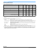
PRESSURE (P1)/VACUUM (P2) SIDE IDENTIFICATION TABLE
Freescale Semiconductor designates the two sides of the
pressure sensor as the Pressure (P1) side and the Vacuum
(P2) side. The Pressure (P1) side is the side containing
silicone gel which isolates the die from the environment. The
Freescale Semiconductor pressure sensor is designed to
operate with positive differential pressure applied, P1 > P2.
The Pressure (P1) side may be identified by using the
table below.
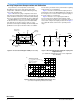
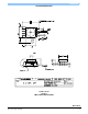
MINIMUM RECOMMENDED FOOTPRINT FOR SMALL OUTLINE PACKAGES
Surface mount board layout is a critical portion of the total
design. The footprint for the semiconductor package must be
the correct size to ensure proper solder connection interface
between the board and the package. With the correct pad
geometry, the packages will self-align when subjected to a
solder reflow process. It is always recommended to fabricate
boards with a solder mask layer to avoid bridging and/or
shorting between solder pads, especially on tight tolerances
and/or tight layouts.
Figure 5. SOP Footprint
Part Number Case Type Pressure (P1) Side Identifier
MP3V5004GC6U/T1
482A
Side with Port Attached
MP3V5004GP
1369
Side with Port Attached
MP3V5004DP
1351
Side with Part Marking
MP3V5004GVP
1368
Stainless Steel Cap
0.660
16.76
0.060 TYP 8X
1.52
0.100 TYP 8X
2.54
0.100 TYP 8X
2.54
0.300
7.62
inch
mm
SCALE 2:1